Institute Nanospectroscopy
Nanostructured Thermoelectrics
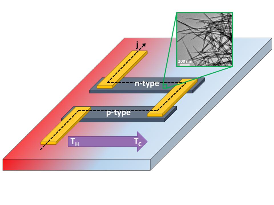
We have several research activities focused on the development of nanostructured thermoelectric materials. Thermoelectrics are a class of materials capable of generating electricity from a thermal gradient. The performance of these materials is typically discussed in terms of a dimensionless figure of merit, ZT=S2σT/κ, where S is the Seebeck coefficient, σ is the electrical conductivity, T is the temperature, and κ is the thermal conductivity. The main idea behind nanostructured thermoelectric materials is that the lattice thermal conductivity of a material can be reduced by means of phonon scattering at nanoscale interfaces. Towards this end, we are developing new materials via microwave-based synthesis approaches, solution-based synthesis approaches, and via sputtering of nanoscale thermoelectric superlattices. These activities are primarily performed within the Energy Materials In-Situ Laboratory Berlin at Bessy II.
A few examples of our research efforts are presented in the following.
For a full list of publications from our institute, please click here.
Nanostructured Hybrid Materials for High Performance Thermoelectrics
Hybrid thermoelectric devices based on conducting polymers and chalcogenide-based nanostructures have been proposed due to the intrinsic low thermal conductivity of the polymer, in addition to pursuing nanostructuring as a means of further improvements via phonon scattering. These hybrid materials systems also offer advantages related to their solubility characteristics, which offer a route towards low cost, solution processable applications. While some work has been done in this context, most of the resulting composite materials are p-type, owing to difficulties in n-type doping of conducting polymers, and the nature of the applied nanocrystals, and there is a strong drive to compliment the advances in hybrid p-type materials with new n-type materials. We have recently developed a new approach for the synthesis of n-type hybrid materials based on Ag2Te encapsulated in PEDOT:PSS, where we are able to directly control the stoichiometry of our Ag2Te during synthesis. We have found that we can effectively tune the majority carrier of this hybrid material system from p-type to n-type. Along with developments in the electronic properties, we are investigating how different synthetic conditions influence the resulting morphology, which can then be related to the thermoelectric performance. We aim to show how these changes in the structure and composition relate to the thermopower and electrical conductivity in an effort to guide performance improvements in these and related hybrid material systems.
Solution-based synthesis of group IV nanoparticles from organo(germanium, silicon) halide precursors
Group IV semiconducting materials, such as Si0.8Ge0.2 have attracted significant attention as high-temperature thermoelectric materials for industrial and space applications. Future directions of interest for these materials include nanostructuring and low-temperature processing. We have developed a solution-based synthesis route that could transform the manufacture of these materials by reducing the energy input required for production. Group IV materials have proven challenging to synthesize colloidally, which has been attributed to their high redox potentials. As an example, the reaction of Ge+4 + 4e- → Ge0 requires +0.12 V. This necessitates the utilization of either high temperatures or strong reducing agents to produce such materials, and these harsh conditions generally make good control over size and crystallinity in one step difficult to achieve. We are currently investigating the relatively low-temperature (300 °C) synthesis of group IV nanoparticles from organo(germanium, silicon) halide precursors in the presence of sulfur, using primary amines simultaneously as solvent and ligand. We have defined a general reaction mechanism that can be utilized towards the synthesis of Germanium, Silicon, and Silicon/germanium nanostructures. This method has the advantages of utilizing benign reagents, low temperatures, and standard bench top chemistry to produce monodisperse nanoparticles.
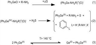
Reaction mechanism for the reduction of organogermanium halide precursors to elemental germanium nanoparticles. Reaction (1): cleavage of the halogen assisted or preceded by amine coordination. Reaction (2): reduction of Ge(IV) to Ge(II) by H2S. Reaction (3): spontaneous disproportion of the Ge(II) over 140 °C to Ge(0) and Ge(IV).
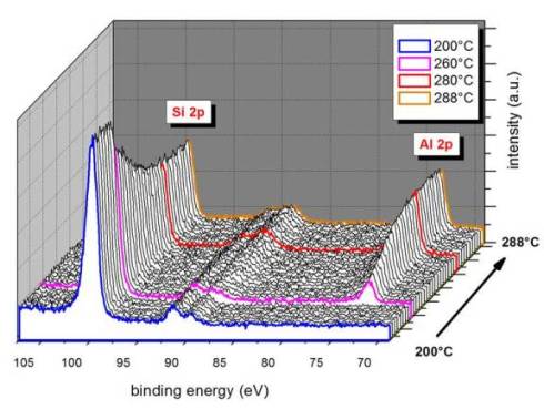
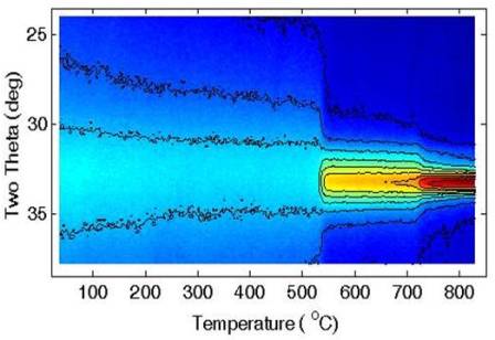
Phase transitions in Ge and Si superlattices by metal-induced crystallization
Polycrystalline Si and Ge thin films find applications in several technologies, including the semiconductor industry, photovoltaics, and thermoelectrics. The quality of the polycrystalline semiconductors is often an essential factor influencing the performance of these devices. Metal-induced crystallization (MIC) for immiscible alloy systems is a process whereby atoms become very mobile due to bond weakening effects at the metal-semiconductor interface and migrate into metal grain boundaries. Due to thermodynamic effects, these mobile atoms crystallize at a much lower temperature compared to bulk materials. This process continues until, at the right film thicknesses, a complete layer exchange occurs. For compound forming metals, on the other hand, crystallization occurs by formation of compounds and the MIC process can go through a subsequent formation of various compounds for some metals. We apply MIC to group IV systems as thermoelectric superlattices, because MIC has been shown to reduce the crystallization temperature of Si, Ge and SiGe substantially for certain metals, notably Au and Al.