Institute Silicon Photovoltaics
Constant Final State Yield Spektroskopie
for the characterization of amorphous silicon
Basics
In contrast to insulators and crystalline semiconductors, amorphous silicon has electronic states not only in the bands, but also in the band gap. They result from strain in the amorphous network and from rupture of Si-Si bonds. At densities below 1020 eV-1cm-3 (as compared to >1021 eV-1cm-3 in the valence band) they are below the detection limit of conventional UPS spectroscopy. Using Constant-Final-State-Yield spectroscopy (CFSYS) [1-3], these densities of states are still detectable. In CFSYS, the energy Ephot of the photons impinging on the sample is he variable, the kinetic energy Ekin where the analyser detects the electrons is the fixed quantity (in conventional UPS, this is the other way round). Ekin is chosen such, that the electrons are detected that are just able to overcome the work function barrier ΦSample from the sample into the vacuum.
Measurement setup
To vary Ephot, a Xe high pressure lamp with double monochromator is used which gives a sufficient photon flux (light intensity) up to ~ 7 eV (near UV). Thus, the energy interval that can be covered with CFSYS ranges from the Fermi edge (Ebind=0) to (Ebind=−7eV−FProbe) at about −3,5 eV. Thus, only states in the band gap (a-Si:H: Egap~1,7 eV) and in the valence band close to the band edge are accessible to the measurement.
Advantage
The advantage of this PES variant lies in the high information depth, i.e. the maximum depth in which a photoelectron can be created that can still exit into the vacuum and be detected by the energy analyzer. At photoelectron energies of 4-7 eV the information depth, which is approximately identical to the mean free path of the electrons between inelastic scattering events λmpf, is ~5-10 nm ². In contrast, for excitation with Ephot=21,2 eV (He I), limpf ~0,5 nm 2. Thus, it is possible to measure an average density of states in the first ~10 nm of a sample. This is ideally suited fort he investigation of ~5-10nm thin a‑Si:H emitter, BSF and passivation layers such as the ones used in a‑Si:H/c‑Si heterojunction solar cells. The density of states NOCC(E) can be measured down to 1015 eV-1cm-3. For very thin a‑Si:H layer thicknesses, the PES spectrum contains additional contributions from the valence band of the underlying c‑Si substrate. Therefore, it is possible to determine the band offset at the a‑Si:H/c‑Si heterojunction from such spectra with a minimum of assumptions [5,6].
2 The reason is, that the low energy of the photoelectrons is not sufficient to excite phonons in the sample material. Therefore, the main inelastic scattering process cannot take place.
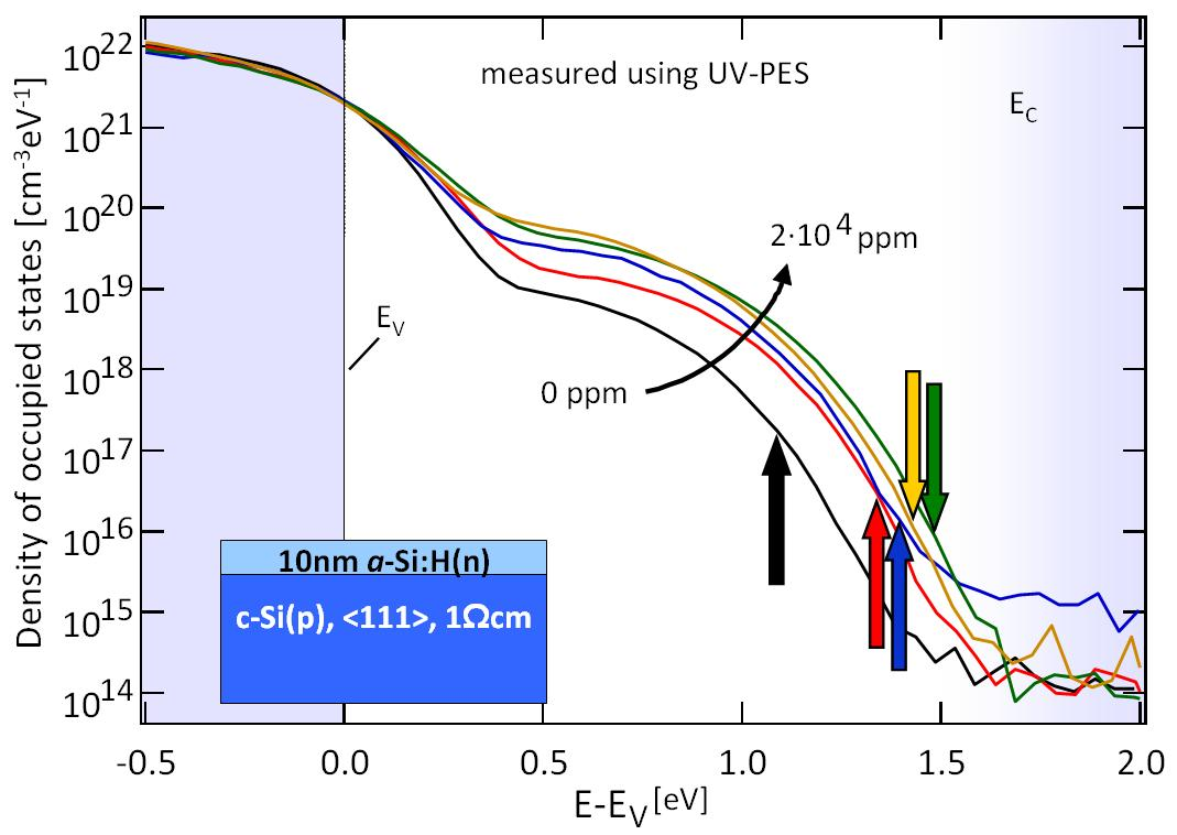
Example of a CFSYS measurement of differently doped, ~10nm thin a-Si:H films on crystalline silicon (c-Si) substrates [6]: EV marks the valence band edge of the a-Si:H. With increasing n-type doping of the a-Si:H, the defect density in the band gap increases, and the Fermi level EF (vertical arrows) moves towards the conduction band edge EC. Electronic states above EF are not visible in photoelectron spectroscopy, since they are not occupied by electrons.
References
|
[1] |
L. Korte; A. Laades & M. Schmidt, J. Non-Cryst. Sol. 352 (2006) 1217-20 |
|
[2] |
M. Schmidt; A. Schoepke; L. Korte; O. Milch & W. Fuhs, J. Non-Cryst. Sol. 338-340 (2004) 211-214 |
|
[3] |
K. Winer & L. Ley, Phys. Rev. B 36 (1987) 6072 |
|
[4] |
L. Korte & M. Schmidt, J. Appl. Phys. 109 (2011) 063714-1-6 |
|
[5] |
M. Sebastiani; L. D. Gaspare; G. Capellini; C. Bittencourt & F. Evangelisti. Phys. Rev. Lett. 75 (1995) 3352-5 |
|
[6] |
L. Korte & M. Schmidt, J. Non-Cryst. Sol. 354 (2008) 2138-43 |