Institute Silicon Photovoltaics
Etching of Si surfaces by chemical or electrochemical processing
1) Metal assisted chemical etching (MACE)
This etching method needs HF/H2O2 solution and a noble metal like Ag, Au, Pt, etc. as catalyst for positive charge injection into the Si surface that leads to the local dissolution of Si [1-4] as sketched in Fig. 1.
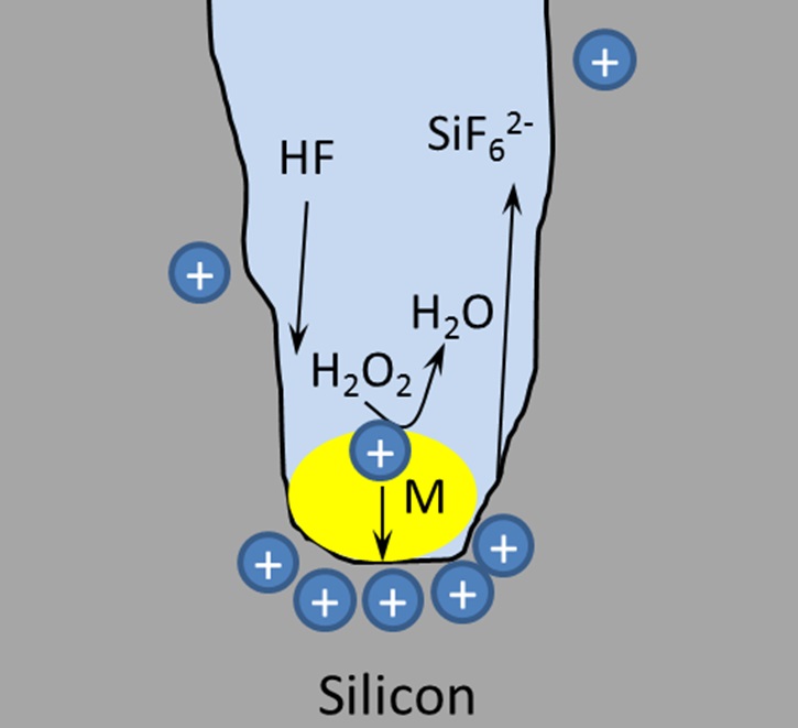
Fig. 1: Sketch of the MACE process, where H2O2 is reduced to H2O at the noble metal particles and the holes are injected into Si that leads to dissolution of Si as SiF62- species (adapted from [1]).
a) Nanoholes and nanowires by random Ag-deposition
Fig. 2 shows SEM images of current-less deposited Pt, Pd, and Ag particles and of an annealed Ag layer randomly distributed on Si surfaces for use in the MACE process. The resulting structures after etching are depicted in fig. 3.
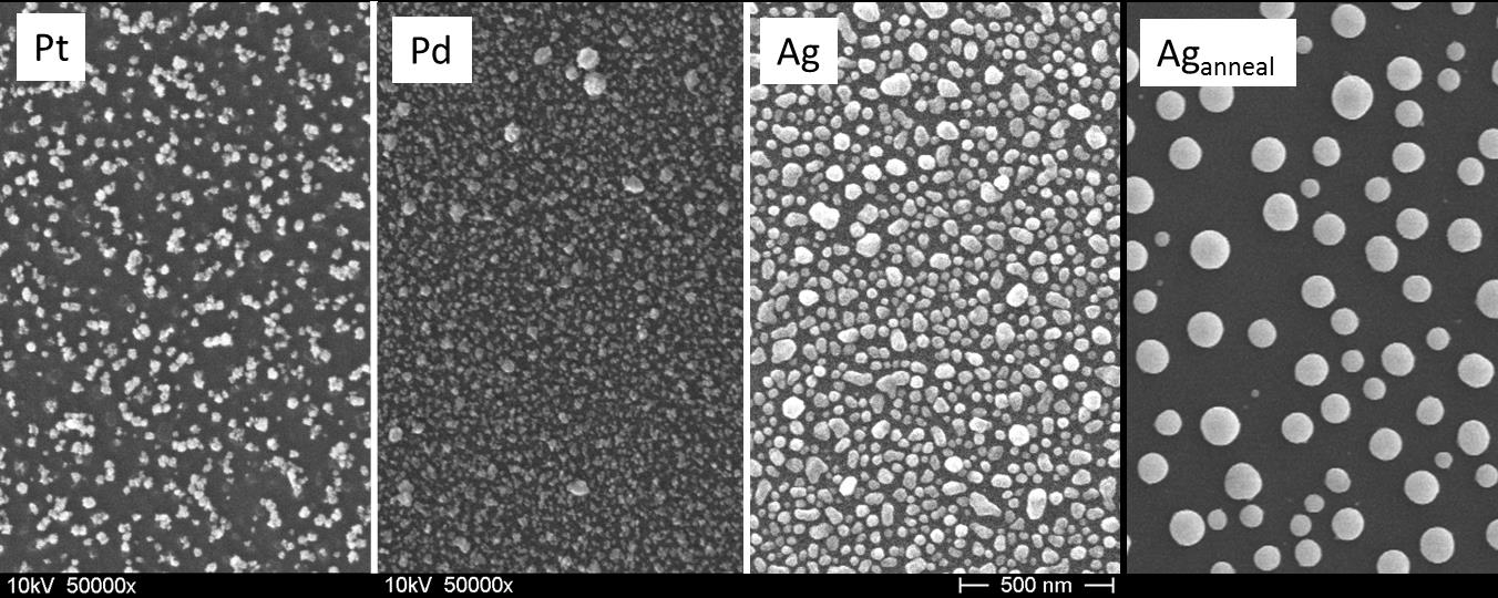
Fig. 2: Pt,Pd,Ag particles on silicon (top),

Fig. 3: resulting structure in silicon substrate after etching (bottom)
b) Regular Si-nanowire structures by nanosphere lithography
This technique provides the possibility to create regular structures of nano- or microwires by using polystyrene templates for the MACE process [4,5] as visualized in Fig. 4 leading to Si-nanowires as presented in Figs. 5 and 6.
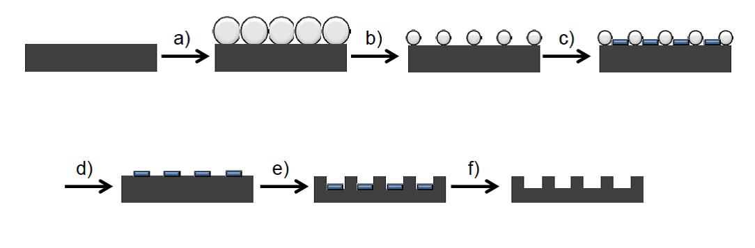
Fig. 4: Mechanism of the MACE procedure in combination with nanosphere lithography. (a) Deposition of polystyrene nanospheres by using a Langmuir-Blodgett trough. b) Reduction of the sphere diameter by reactive ion etching (RIE) in oxygen plasma. c) Deposition of the metal catalyst. d) Removal of the polystyrene spheres. e) Exposure of the sample towards an etching solution resulting in nanowire formation. f) Removal of the metal catalyst

Fig. 5: Side view of Si-nanowires obtained with 1 µm polystyrene spheres downsized by RIE in different magnifications of the SEM (a: 1000x, b: 2000x, c: 10000x, same as c but top view).
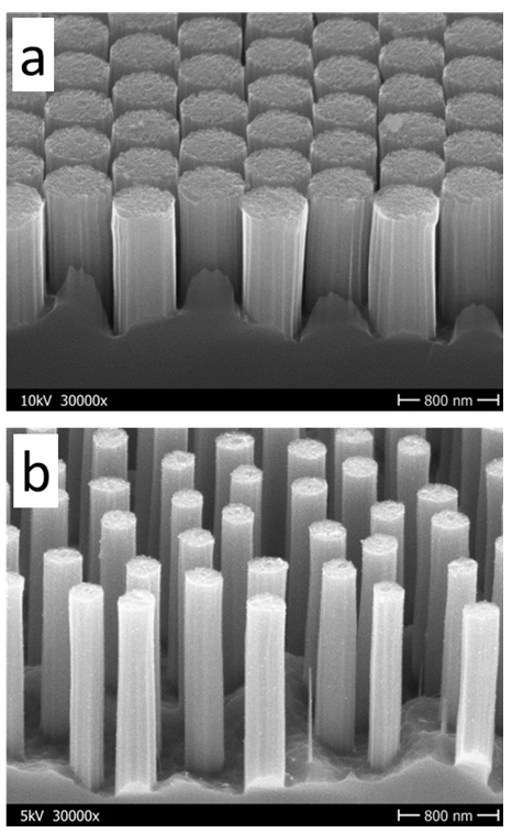
Fig. 6: SEM side views of Si-nanowires obtained with 500 nm polystyrene spheres (top) and downsized by RIE (bottom).
2) Light scattering layers
Fig. 7 shows SEM images of electrochemically etched Si (J, K) and µc-Si surfaces (A, B, C) in comparison to a nanowire-structured Si surface (NW). The respective diffuse reflection spectra of these samples are presented in Fig. 8 [5-7].
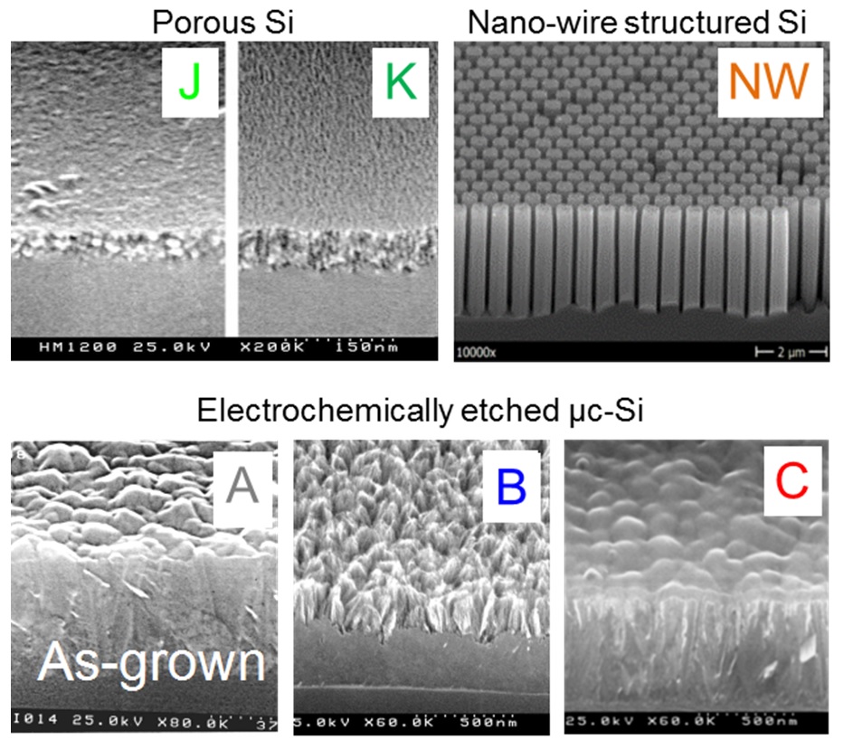
Fig. 7: Thin nanoporous layers on c-Si etched in 10 % HF:Ethanol at 5 mA/cm2 for 0.5 min (J) and 1 min (K); As-grown µc-Si layer on Si (A) and nanowire-like layer of µc-Si etched in 5 % HF:Ethanol at 2.5 mA/cm2 for 0.5 min (B) and similar etched µc-Si layer covered additionally with a 50nm thick anodic SiO2 layer (C), and a nanowire-structured Si surface as prepared by MACE (NW).

Conclusion: A thin electrochemically etched Si surface layer (about 60 nm) is able to reduce diffuse reflectance strongly without the consumption of great amount of the deposited Si. The reflection loss is more strongly reduced by the nanowire-like structure than by porous layers on c-Si. Also the nanowire-structured surface has a strong reduction in the diffuse reflectance.
References
[1] Metal-assisted chemical etching of silicon in HF–H2O2; C. Chartier, S. Bastide, C. Lévy-Clément, Electrochimica Acta 53 (2008) 5509-5516
[2] Ordered nanopore boring in silicon: Metal-assisted etching using a self-aligned block copolymer Au nanoparticle template and gravity accelerated etching; S. Bauer, J.G. Brunner, H. Jha, Y. Yasukawa, H. Asoh, S. Ono, H. Böhm, J. P. Spatz, P. Schmuki; Electrochem. Communications 12 (2010) 565–569
[3] Metal-Assisted Chemical Etching of Silicon: A Review; Z. Huang, N. Geyer, P. Werner, J. de Boor, U. Gösele; Adv. Mater. 23 (2011) 285-308
[4] Electropolishing and passivation of silicon nanowires towards hybrid interfaces; J. Hänisch, C. Klimm, J. Rappich; Electrochimica Acta 226 (2017) 46–52
[5] Preparation of Thin Nanoporous Silicon Layers on n- and p-Si; Th. Dittrich, I.Sieber, S. Rauscher and J. Rappich; Thin Solid Films 276, 200-203 (1996)
[6] Light trapping by formation of nanometer diameter wire-like structures on µc-Si thin films; J. Rappich, S. Lust, I. Sieber, W. Henrion, J.K. Dohrmann, and W. Fuhs; J. Non‑Cryst. Solids 266, 284‑289 (2000)
[7] Electrochemical microstructuring of silicon thin films for use in light trapping systems; S. Lust, J. Rappich, I. Sieber, W. Henrion, W. Fuhs; Proc. of the 16th Europ. Conf. on Photovoltaic Solar Energy Conversion, Eds.: H. Scheer, B. McNeli, W. Palz, H. A. Ossenbrink, P. Helm, James & James Ltd, London, UK (2000) 1309-1312