Institute Silicon Photovoltaics
Embedded graphene for large-area silicon-based devices
In this project we investigated the possibility to embed graphene with an amorphous Si layer followed by laser crystallization process where the graphene successfully withstand such high temperature processing (see red line in Raman spectra Fig. 6 left) with slight changes in electronic quality (see red triangles in the Hall measurement Fig. 6 right) [6].
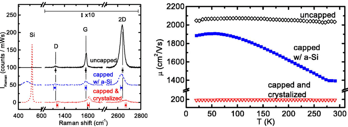
Fig. 6
references
[6] Embedded graphene for large-area silicon-based devices; Gluba, M.A.; Amkreutz, D.; Troppenz, G.; Rappich, J.; Nickel, N.H.; Appl. Phys. Lett. 103 (2013) 073102.