Innovation Lab HySPRINT
2D/3D Integration Processes
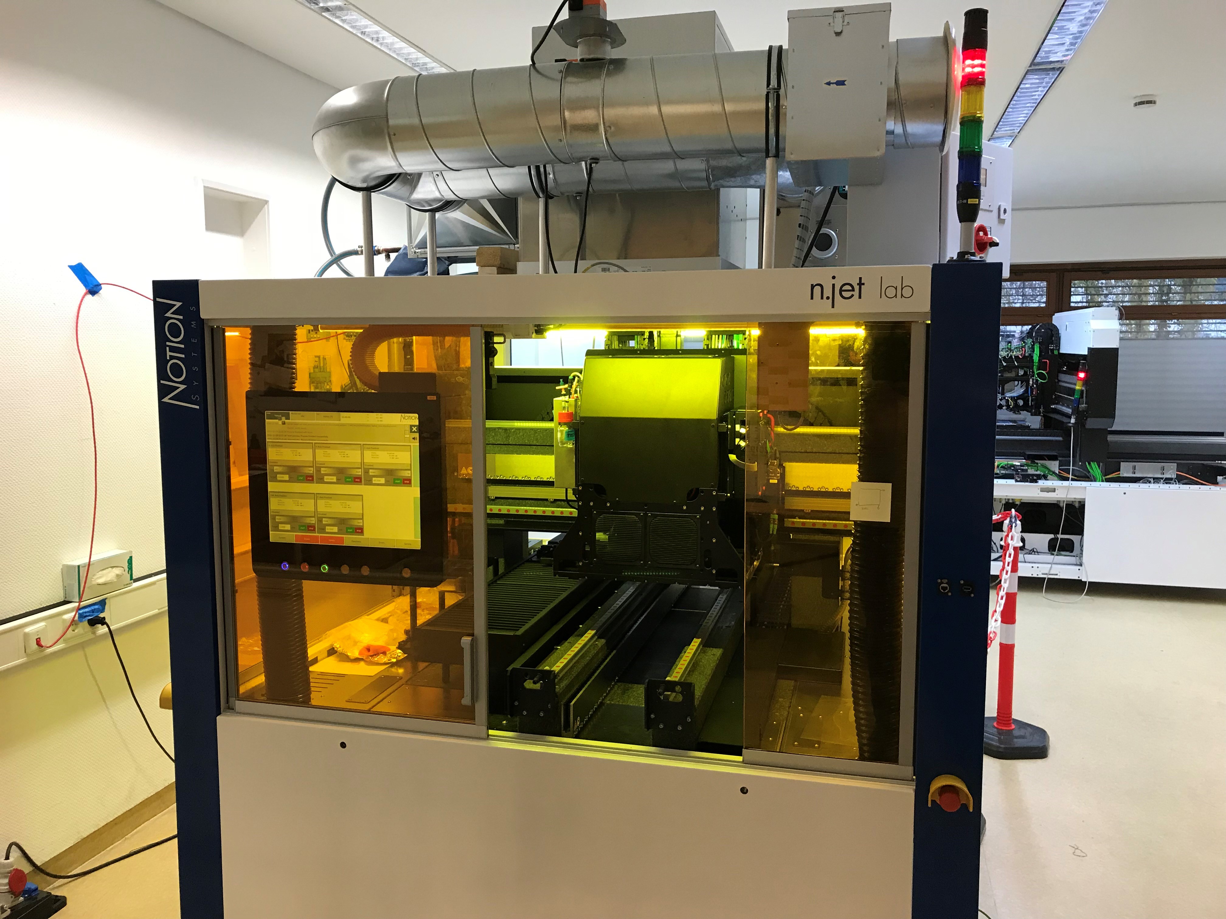
Notion Systems Maschine for Inkjet Printing (Foto HZB)
Inkjet Printing of Electronics
The use of solution-processable materials for the fabrication of electronic and optoelectronic devices enables the implementation of scalable processing techniques such as printing. As opposed to techniques used to coat entire surface areas, by printing it is possible to directly write arbitrary patterns on a variety of surfaces without the need for masks or structural pre-patterning.
Within our labs of both GEN_FAB and Hybrid Devices, we implement printing processes for a range of material classes, such as conductive inks and polymers. We investigate ink parameters such as viscosity and surface tension and understand surface properties through contact angle measurements. By understanding these properties, we can influence the printing parameters, while through appropriate post-processing, the printed material is then turned into a fully functional material.
Through the use of multiple printheads we are able to produce several inkjet-printed layers within a single machine. Additionally, we use combinatorial approaches through multiple printhead inkjet printing to screen inks and optimize ink compositions.
Finally, we use 3D printing in the form of fused deposition printing and stereolithography to allow us to produce complex custom parts for our scientific setups.
Contact: Prof. Dr. Emil List-Kratochvil
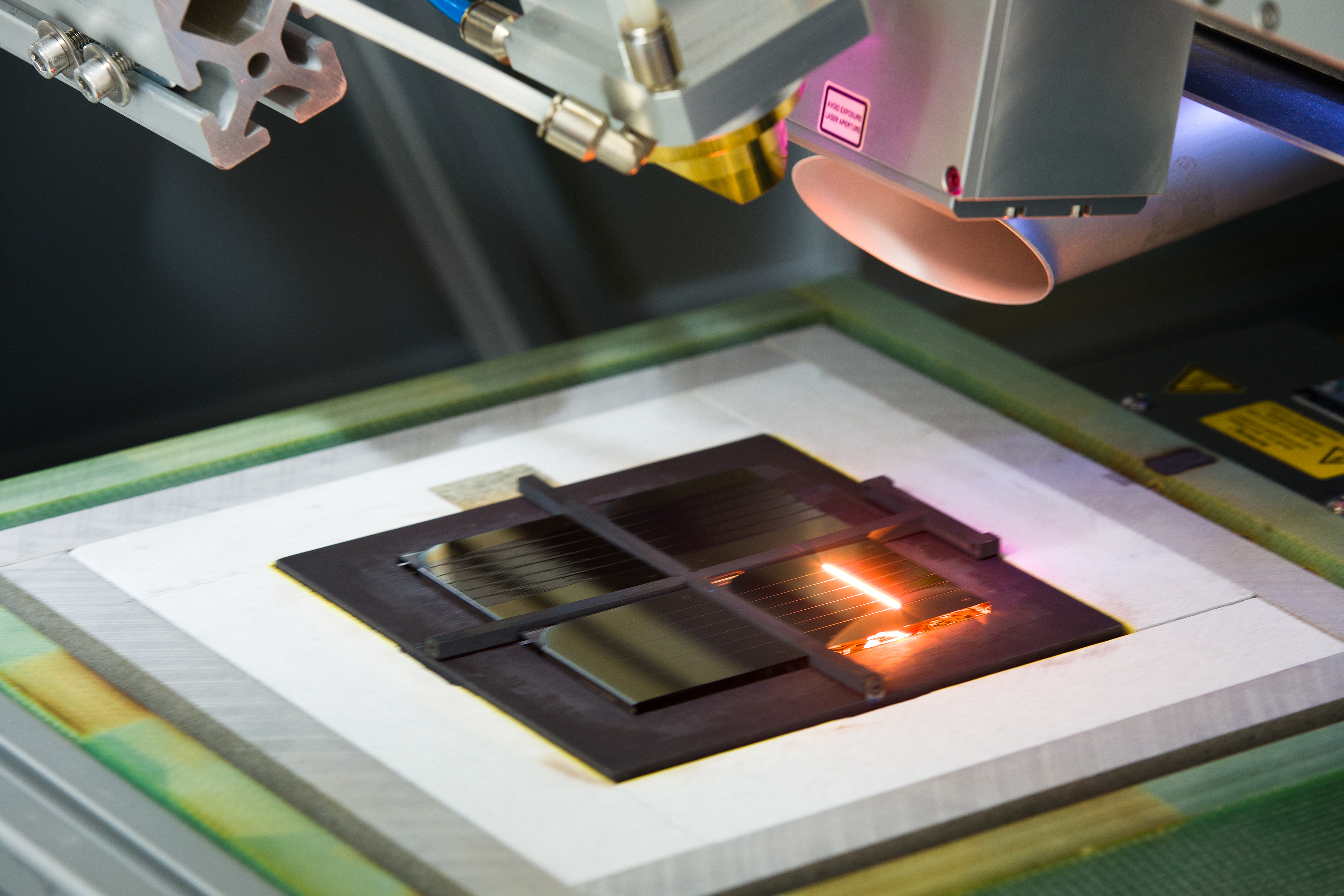
Laserline Source for the Material Finishing and Silicon-on-Glas Technology
The recent progress in the field of high power diode lasers and LED illumination lead to novel beam sources that combine high power densities, excellent conversion efficiencies with flexible beam geometries and wavelengths. The focus of this project is the evaluation of these sources for applications in the field of PV, display technology or sensors and to contribute to the further development of these sources. The established deposition technology at HZB enables for example a direct crystallization of silicon on glass without the need for time and energy consuming dehydrogenation processes. The increasing availability of diode laser sources emitting a short wavelength (450nm) enables tailored annealing processes or crystallization of ultra-thin silicon layers for thin-film microelectronics or transparent conductive oxides (TCOs).
Contact: Dr. Daniel Amkreutz
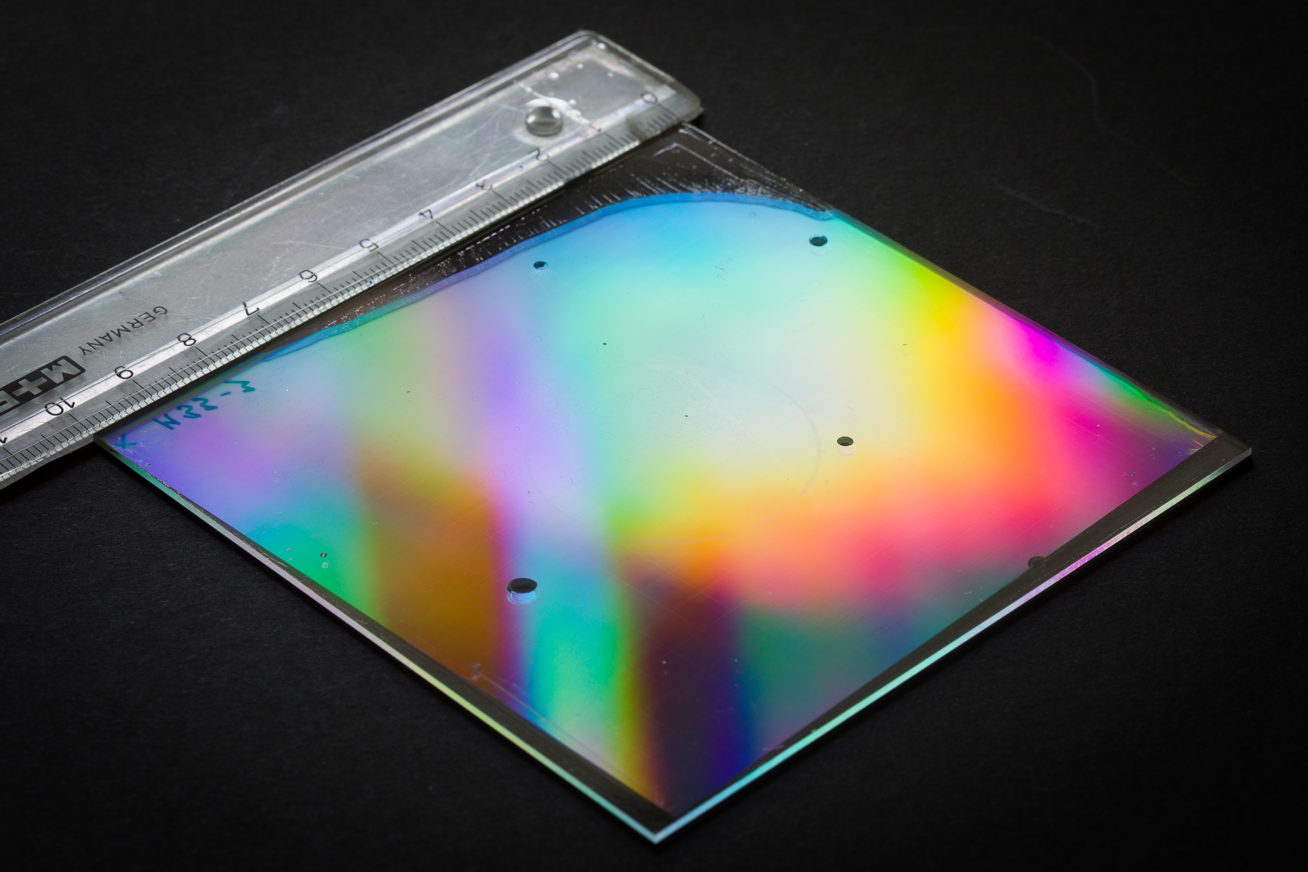
Nano-Imprint Lithography
We work on developing and characterizing large area photonic crystals and light management structures, which can be applied for biosensorics / gas sensors, solar energy conversion and spectral conversion. For the development, we combine numerical calculations and optimizations with nanoimprint lithography for the production of nanostructures in the laboratory. On focus will be to scale the nanostructuring method to areas up to 10 × 10 cm2.
Contact: Prof. Dr. Christiane Becker