Innovation Lab HySPRINT
QYB Quantum Yield Berlin - Spin off story
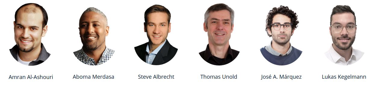
The QYB founders
“Our mission is to make research easier and more efficient”
By Kai Dürfeld
Making electronic components more efficient conserves natural resources, reduces costs, and helps the environment. With their newly founded spin-off company QYB Quantum Yield Berlin, six researchers from the Helmholtz Zentrum Berlin (HZB) want to provide their colleagues the world over with a device that will make their research work more efficient.
Solar cells need to convert as much energy from sunlight into electrical power as possible. LEDs, on the other hand, should consume as little electrical energy as possible and emit a maximum amount of light. To achieve this, scientists are working in laboratories all over the world to improve the materials and design of these optoelectronic components. This is sometimes tedious and requires many hours of processing and measurement time. A team from the Helmholtz Innovation Lab HySPRINT at the Helmholtz-Zentrum Berlin (HZB) now wants to shorten this process. With their new company QYB Quantum Yield Berlin, the scientists are ready to market a device barely the size of a shoebox that will make measurements faster and more convenient. Three of the founders – Lukas Kegelmann, Thomas Unold, and Amran Al-Ashouri – talk about their path to the start-up, why founding a company requires a change of perspective, and how they want to make the world a little bit better.
How did you come up with the idea of founding a company?
Unold: “My research group at HZB has been using this measurement method for a long time. It goes back to the 1980s and was originally applied to silicon components. We have concentrated on adapting, developing, and optimising it for other materials over the last 10 years. Lukas and Amran together with José Márquez, Aboma Merdasa, and Steve Albrecht at the HySPRINT laboratory (an HZB research platform for industry) have established the method for use in high-throughput materials research. In addition, we have also been able to generate great research results with this measurement method in close collaboration with Prof. Neher's group at the University of Potsdam.“
Kegelmann: “That’s right. We have quickly seen the new insights this method of analysis allows us and how much it helps us in our own work – how much time we save, and how much material we save. Simply put, it is because we get meaningful results much faster and thus know faster where there is a problem in our component fabrication. At the same time, we saw how other researchers in the lab enthused about it. A lot of people were interested in the measurement method and applied it to their projects. So we decided that we should provide this capability to other research labs as well – as a simple finished product with integrated software and data analysis, so that the operator can get meaningful data very easily. We developed a market-ready prototype and subsequently founded a company. Thomas, Amran, Aboma, José, and Steve are on board as directors with me as managing director. Our colleagues from the University of Potsdam are also involved as advisors.“
Your measuring device is meant to help to make solar cells and LEDs more efficient. How does that happen?
Kegelmann: “We measure the absolute luminescence efficiency of a semiconductor. That means how much light it can emit when it is in an excited state and has free charge carriers available. To do this, we excite the semiconductor – either by illuminating it with a laser or by sending an electrical current through it. Then we very accurately measure the amount and wavelength of light emitted by the excited semiconductor. We can calculate the absolute luminescence efficiency from the ratio of the emitted light to the incident laser light or injected electrical current. The analysis method is based on this principle and in addition takes into account the physics of the semiconductor device. This allows us to calculate even more detailed physical parameters and quality attributes.
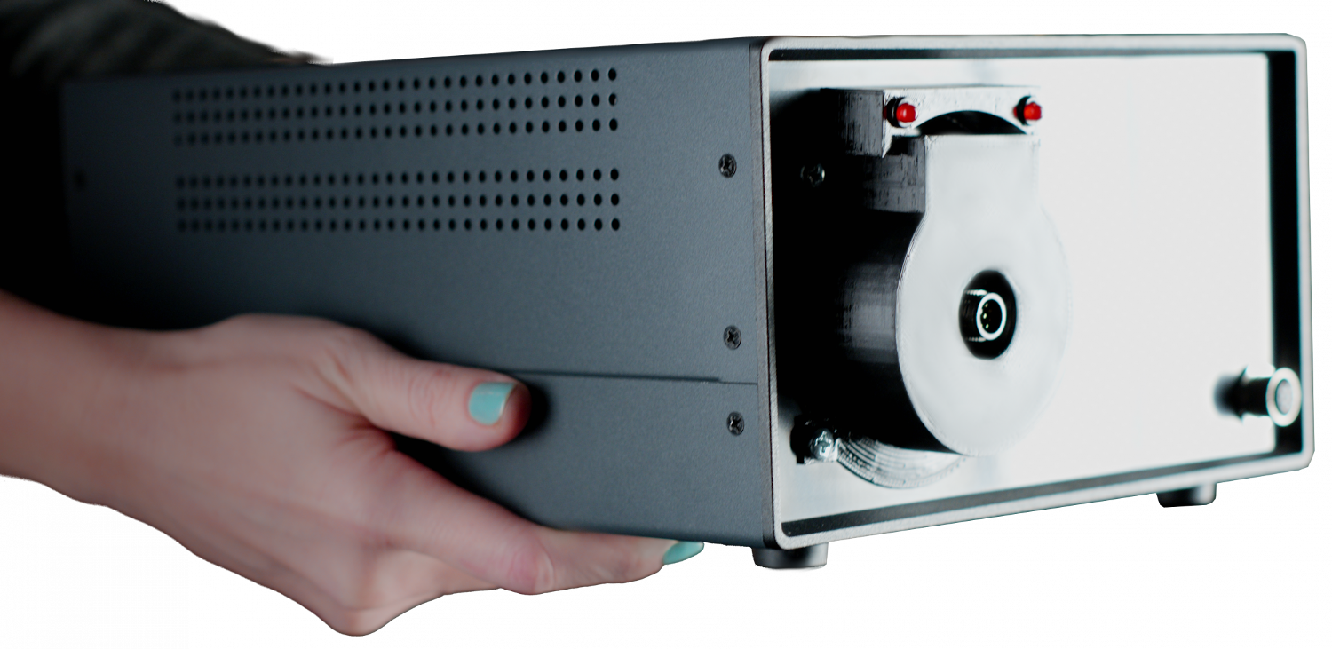
LuQY Pro: Fast, precise and non-invasive measurement of semiconductor characteristics facilitates resource-saving development and optimisation of thin-film solar cells and LEDs
Developing a product and founding a company sounds like a lot of challenges. Did anything cause you sleepless nights?
Kegelmann: “Yes - transforming the laboratory prototype into a market-ready device that works both reliably and stably. That proved to be a bigger challenge than we initially thought it would be. We had to lay out the components properly so they would remain reliable, yet package it as a compact unit. Technical problems cropped up repeatedly and more than once we thought: Oh man, will we be able to solve this, or is this project going to fall apart? But one or two weeks later, the world looked completely different again. What doesn't go away, however, is this general feeling that you taking a certain risk with product development and the step towards forming and operating your own company. There is always the danger that it won't work out in the end the way you imagined. That can be intimidating.“
Al-Ashouri: “For me, it was the change of perspective that was challenging – and exciting at the same time. Suddenly we had to express our goals and our selling points in a completely different way. We had to sell ourselves differently than when we argue for pure science. This is because we scientists normally ponder things, somewhat isolated in our own world of the laboratory. And suddenly we had to look outwards. We had to consider whether what we had developed was really useful. And how to sell it. Also, scientists sometimes build up an almost loving relationship with their experimental set-ups. It shows in the care with which we use them. However, as an entrepreneur, you have to keep in mind that customers will not use your device as carefully as you do. Mistakes will also happen. This is a learning process for us and we have already learned a lot – because when twenty-five or so different people use the device here in the HySPRINT Lab, some unforeseen things happen.“
Unold: “The challenges are definitely diverse, but I would also like to put them into perspective a bit. For me, this is already a success story. It shows what is possible to achieve, if you want to. When Lukas came to me and said what he wanted to do, I didn't really know what to think. There are always ideas that very quickly come to nothing. I myself have participated in earlier technology transfer projects that ultimately did not make it to the spin-off stage. This is because it doesn't take just a good idea. The market must also be ready for it. The composition of the team has to be right and the driving forces have to be brought to bear. In this case, everything came together. In addition, the support from the HZB Technology Transfer Department was very good in my view. I have no doubts today. On the contrary: I am really thrilled.“
Kegelmann: “That's a good way to put it. At this point, I would also like to praise the cooperation we received from the Technology Transfer Department at HZB. It was totally straightforward and really helped us enormously, not only with advice and know-how on product development and founding a company. There are also ideal funding instruments, such as the Technology Transfer Fund and the Field Study Fellowship. Without this funding, we would hardly have had any financial leeway and probably wouldn't have taken the risk of building a prototype in the first place.“
What is your mission as an entrepreneur? How do you want to make the world a little bit better?
Al-Ashouri: “That's a very good question. We discussed it at the very beginning when Lukas had the idea of founding a company. I wouldn't be on board if he was only interested in making money. What we're really about is something every scientist notices when working in a lab: a lot of resources are needed to do research – consumables as well as large amounts of electrical power. You consume these resources every day you step into the lab. On the other hand, we researchers are seen as people who want to make the world a little better. And that's exactly where we come in. Using our device, a single day in the lab is enough to discover the optimum composition for a given semiconductor – not five days, as has been the case up to now. This not only saves time, but also conserves valuable resources, and for me it is the reason why I am involved.”
Kegelmann: „Amran has hit the nail on the head. The measurement method is fast, simple, and non-invasive – it does not alter the sample. It provides not just new insights, but also saves an enormous amount of time and resources. Making this capability available to other laboratories is the main motivation for me as well.”
Unold: “We have worked a lot over the last ten years in my group to make research more effective and more focussed. So it is also my very personal mission. That's why I'm very pleased that our efforts are finding resonance, and that the new product will hopefully be employed in an ever larger research group, too.”
What does the future hold for QYB?
Al-Ashouri: “The prototype will stay here at the HySPRINT lab and continue to be used. It is very popular in the lab. And it gives us the advantage of continuing to accumulate experience with it. We will be building new instruments for our customers, of course. But it won't be mass production for the time being. We don't expect to sell more than ten units a week at present. Not yet, anyway”, he laughs.
Kegelmann: “That’s right – but seriously, we will actually manufacture the first commercial devices in a small workshop. At the same time, we still have access to the HySPRINT laboratory. That's the nice thing. We have beta testers there, and our prototype has already been tested there during development. We always received quick feedback that we could incorporate in the prototype.“.
And where do you see your company in three years?
Kegelmann: “We want to sell the first device by this summer. In three years at the most we will have established additional products. We are already receiving requests to expand the functionality of the system even further in order to be able to evaluate several semiconductors simultaneously. This is interesting, for example, for the development of so-called multi-junction solar cells. At the same time, our company will grow and portions of the production or even all the production will be outsourced. We can then concentrate on expanding the product portfolio and the customer base."