Innovation Lab HySPRINT
INDUSTRY DAY at HZB - Optoelectronics / Photovoltaics

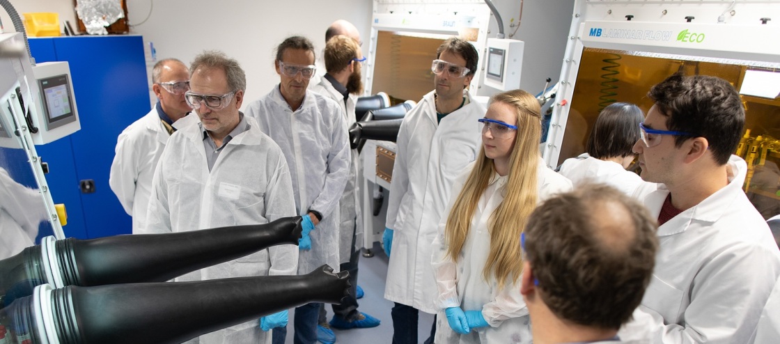
HySPRINT Perovskite-Lab (Foto: HZB/Michael Setzpfandt)
Fruitful networking at HZB Industry Day: Shaping the future of optoelectronics and photovoltaics with industrial partners
01.04.2019
On 28th March, Helmholtz-Zentrum Berlin invited industry key players in the fields of optoelectronics and photovoltaics to an industry day in Berlin-Adlershof to discuss around the key topics material and components development, analytics and simulation.
More than 50 participants had the opportunity to get an overview about the technology transfer activities driven by the competence centre of thin film and nanotechnology for photovoltaics Berlin (PVcomB) and the Helmholtz Innovation Lab HySPRINT at HZB.
After a short welcome by HZB scientific managing director Prof. Dr. Bernd Rech and an introduction to technology transfer by PVcomB director Prof. Dr. Rutger Schlatmann, HZB leading experts presented successful cooperations with our industry partners Avancis, Creaphys M.Braun, JCM Wave, LIMO, Oxford PV and Von Ardenne.
They showed that partnerships between HZB research and industry are leading to marketable technologies or devices. Collaboration with research institutions is, indeed, fruitful for the companies. For instance, Von Ardenne implemented this technology for application in solar cells together with PVcomB and HySPRINT. “By combining our experience with that of our partner, we are well positioned to develop and manufacture industrially relevant, stable transparent conductive oxides (TCOs) for photovoltaic devices.”Dr. Darja Erfurt from HZB says.
During the networking session, industry guests discussed with our experts challenges and opportunities of the industrial development of optoelectronics and photovoltaics. Dr. Sven Burger from JCMwave GmbH states “We are collaborating with HySPRINT on the topics of exploiting optical resonances for energy applications. The project spans the technology readiness levels from basic research on numerical algorithms (TRL 2) to software validated by national institutes of standards and by industrial customers (TRL 8-9). Also, together with our HySPRINT partners we successfully obtained BMBF funding for a research project which would be hardly possible without our cooperation within HySPRINT.” Christopher Kerth (transfer and innovation at Helmholtz Association), confirmed “The event inspired us to invest more into getting the right people together.”
The Industry Day concluded by the HySPRINT perovskite lab as well as the silicon and CIGS labs at PVcomB opening their doors to give our guests an insight into our state-of-the-art R&D infrastructure and equipment.
Helmholtz-Zentrum Berlin operates the Helmholtz Innovation Lab HySPRINT and PVcomB to accelerate the transfer of optoelectronic and photovoltaic technologies.
The industry day took place in cooperation with WISTA Management and with the support of Berlin Partner for Business and Technology as well as Brandenburg Invest (WFBB).
We look forward to the next industry day 2020.
Presentations (German) can be downloaded here.