Innovation Lab HySPRINT
Silicon Lab
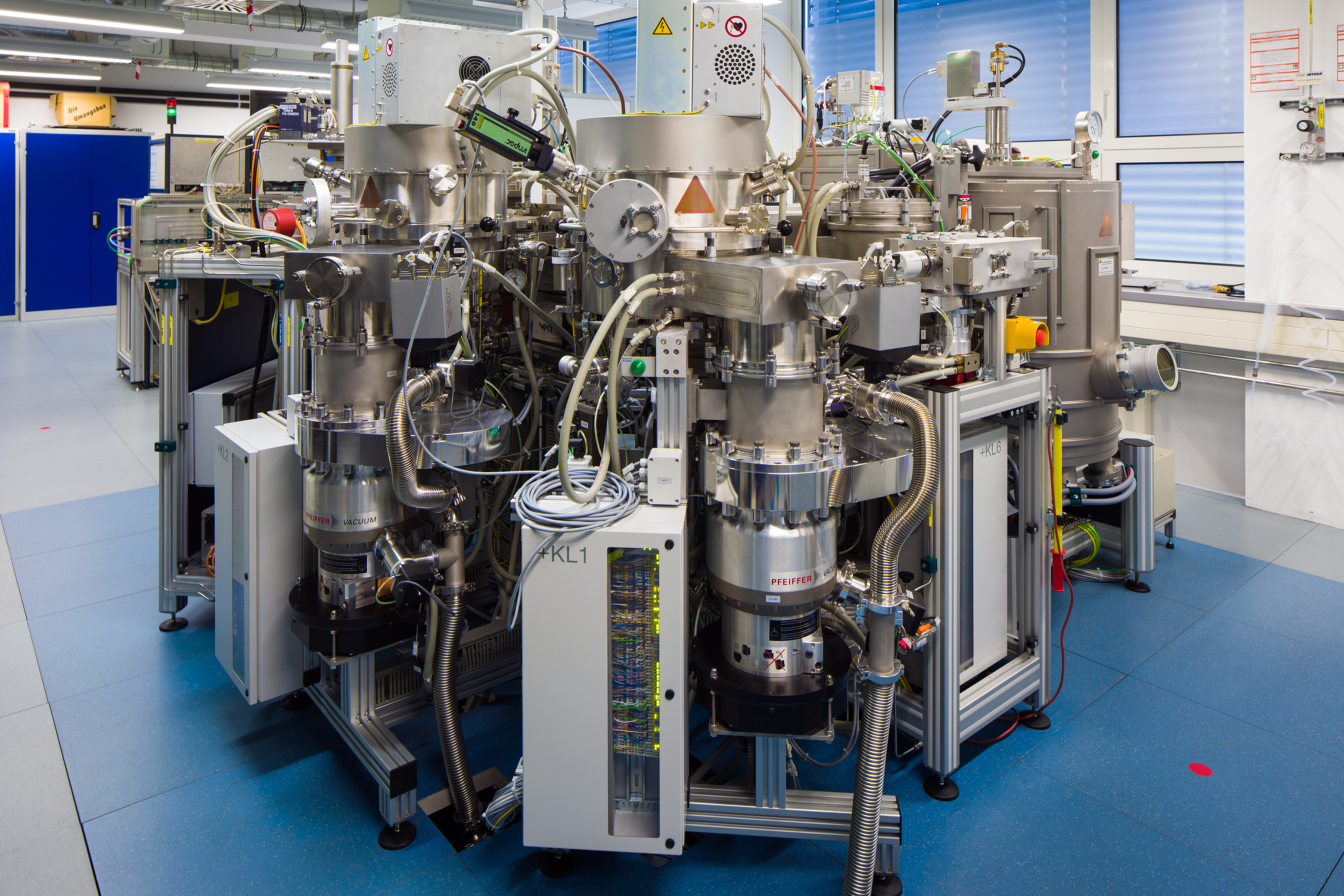
The silicon lab offers different tools for the deposition and post-treatment of thin-films. For the preparation of precursor layers for our liquid phase crystallization technology, an integrated PECVD / PVD cluster is available. Our Von Ardenne CS400PS cluster is equipped with two PECVD chambers, one rf-magnetron sputter source and two high rate electron beam evaporators for silicon deposition. In addition, the cluster is equipped with a process chamber for hydrogen plasma treatments of silicon-related materials. The cluster offers a fully automated deposition on multiple substrates including face-up and face-down deposition. In addition, a RTA (rapid thermal annealing) furnace and a lasercrystallization system in vacuum is available.