PVcomB
News archive
PVcomB @ EUPVSEC 2017
The world's largest photovoltaic scientific conference takes place from 25-29 September this year in Amsterdam. As in the last years, scientists from PVcomB will present their latest results in PV R&D and discuss the recent developments and technological challenges with colleagues from worldwide research and industry.
If you like to meet us in Amsterdam to discuss scientific questions or if you are looking for a reliable partner in a joint project, don't hesitate to contact us by info@pvcomb.de.
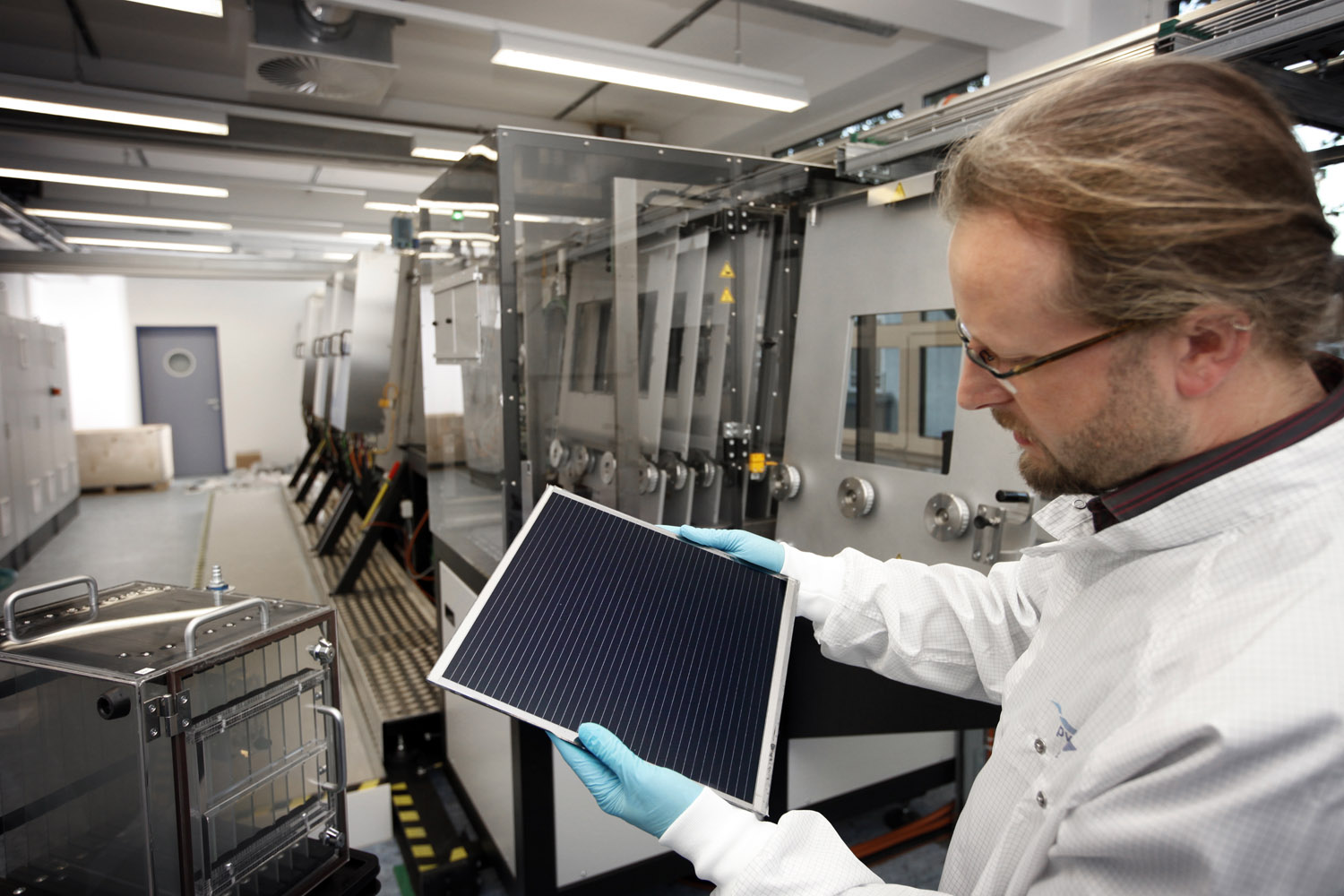
Silicon heterojunction solar cell baseline with certified 22.5 % cell conversion efficiency
Silicon Heterojunction solar cell from the PVcomB Baseline with 22.5% conversion efficiency certified by ISFH CalTeC.
The PVcomB baseline process for industrial silicon heterojunction (SHJ) solar cells has achieved state-of-the-art level, yielding cell efficiencies above 22 %. In less than two years we reached a new milestone. The ISFH CalTeC now certified an efficiency of 22.54 % for a 4 cm² SHJ cell from the PVcomB baseline. Full-size cells (156 x 156 cm²) are being optimized and already reach conversion efficiencies well above 20%.
Silicon heterojunction (SHJ) solar cells are made of crystalline silicon wafers using passivated contacts for both polarities based on i/n and i/p stacks of thin-film silicon alloys, such as amorphous silicon (a-Si:H), nanocrystalline silicon (nc-Si:H) or silicon oxide (nc-SiOx:H). Due to a high silicon wafer (Cz-Si) quality and the excellent surface passivation SHJ solar cells reach very high conversion efficiencies with highest open circuit voltages >740 mV and low temperature coefficient <0.3 %/K. For commercial production, the lean process sequence consisting of only four major process steps, all below <200°C processing temperature, facilitate low-cost cell production. Recently, Kaneka Corp. (Japan) attracted attention with 26.6 % for an all-rear-side contacted (IBC) SHJ cell (world record for a silicon-based solar cell), demonstrating the high potential of the SHJ technology [1].
The Silicon PV Group at PVcomB we develop SHJ cells with the focus on improving industrial applicable materials and processes.
By combining the strong background in thin-film technology at PVcomB with the existing know-how of the HZB institute of silicon photovoltaics and introducing the industrial screen-printing technology for grid metallization we set up an industrial-type baseline process in rather short time. Besides direct applications in industry the SHJ technology is very attractive for various future types of solar-energy conversion devices. Therefore, at HZB we adressing the following research topics:
- New processes to be implemented for high-efficiency SHJ cells in cooperation with PV industry.
- SHJ bottom cell in novel high-efficiency multi-junction (“tandem”) cells, e.g. with perovskite top cells.
- PV cells and modules adapted for hydrogen generation (“solar fuels”).
- Advanced silicon-based passivating contact layers for novel types of silicon-based solar cells, such as liquid-phase crystallized silicon (LPC-Si) solar cells on glass.
References
[1] “Silicon heterojunction solar cell with interdigitated back contacts for a photoconversion efficiency over 26%”, Kunta Yoshikawa, Hayato Kawasaki, Wataru Yoshida, Toru Irie, Katsunori Konishi, Kunihiro Nakano, Toshihiko Uto, Daisuke Adachi, Masanori Kanematsu, Hisashi Uzu and Kenji Yamamoto, NATURE ENERGY 2, 17032 (2017) DOI: 10.1038/nenergy.2017.32.

Fig.: Silicon Heterojunction solar cell from the PVcomB Baseline with 22.5% conversion efficiency certified by ISFH CalTeC. (photos: HZB)
PVcomB will help mass-produce the raw photovoltaic materials used in Wysips® technology (Jan 2017)

Sunpartner Technologies and Helmholtz-Zentrum Berlin sign license agreement
The French company Sunpartner Technologies has been developing innovative solar solutions for nearly 10 years. One of these is Wysips,® an invisible or transparent photovoltaic film that transforms any surface into a solar panel that can generate electricity using the sun’s light. To create Wysips® Crystal and Wysips® Reflect, Sunpartner Technologies paired with the German research centre Helmholtz-Zentrum Berlin (HZB) to develop a special solar material that could be integrated into the company’s technology.
The Wysips® Crystal component is an ultra-thin, transparent glass that combines photovoltaic material with an optical system adapted to display screens like those used in cell phones and connected watches. The component provides the device with a constant power reserve, ensures that certain applications work properly, and independently powers certain operations. For example, exposing a phone to the sun for three minutes will give you one minute of call time.
The goal of Wysips® Reflect is to make connected watches last as long as possible in between recharges. It extends battery life by up to 50% on products it has been applied to, depending on product energy use. The component is completely invisible and can be integrated into a digital or analog watch without affecting its design.
The Competence Centre Thin-Film- and Nanotechnology for Photovoltaics Berlin (PVcomB) at Helmholtz-Zentrum Berlin (HZB) is a trusted supplier of photovoltaic cells and was involved in developing one of the key building blocks in these two Wysips® components: a special photovoltaic material compatible with the transparency process developed by Sunpartner Technologies.
HZB relied on Sunpartner Technologies’ specifications to determine the stacking order that makes up the special photovoltaic material, the quality and thickness of the glass substrate, the formats, and the tolerance levels for cleanness and dust. The result is a turnkey solution, called a “photovoltaic stack,” that Sunpartner Technologies renders transparent or invisible to the naked eye by means of its own proprietary processes.
The French company, whose production unit is located in Rousset, is currently preparing to mass-produce its components. The company and HZB therefore signed a license agreement that allows Sunpartner Technologies to use HZB’s expertise to develop Wysips® Crystal and Wysips® Reflect.
Franck Aveline, VP Consumer Product Line at Sunpartner Technologies, said, “We are very pleased with our collaboration with the Helmholtz-Zentrum Berlin laboratory. They sought to understand us and meet our needs by sharing their expertise and technical abilities with us in the field of thin photovoltaic film. This agreement is a new step we’re taking together towards industrializing Wysips® solutions while still maintaining control of the key technological building blocks we need to develop.”
Bernd Stannowski, senior scientist at HZB, said, “This collaboration allows us to bring our high-efficiency thin-film silicon solar cell technology developed over the past five years to industrialization. With Sunpartner we found an ideal partner to further develop and transfer to production.”
About Sunpartner Technologies
Sunpartner Technologies develops and integrates innovative and invisible photovoltaic solutions for the consumer electronics (wearables, mobile devices, connected objects), building (Smart Cities), and transportation (automobile, aviation, maritime) markets. Its Wysips® technology (short for “What You See Is Photovoltaic Surface”) captures solar energy and converts it to electricity so that ordinary objects require no or almost no outside energy source. The company puts its expertise to work to create smart, attractive surfaces around the world. Sunpartner Technologies was founded in 2008 in Rousset, France, and today has 65 employees and a large portfolio of patents. The company has raised 45 million Euros since its creation.
Speeding up CIGS solar cell manufacture
The funding will go towards optimising a co-evaporation process at PVcomB used for producing CIGS layers for thin-film solar cells. Photo: HZB
The CIGS thin film photovoltaics can be integrated pleasingly into building architectures. Photo: Manz AG
Speeding up CIGS solar cell manufacture
A project consortium from research and industry involving the Competence Centre for Photovoltaics Berlin (PVcomB) of Helmholtz-Zentrum Berlin has been granted a major third-party-funded project by the Federal Ministry of Economics. The project “speedCIGS” is to be funded with 4.7 million euros over four years, of which 1.7 million goes to HZB. The project partners will use this money to accelerate the manufacturing process for CIGS thin-film solar cells and thus make the technology more attractive to industry.
The speedCIGS project is being carried in cooperation with systems builder Manz AG, the Center for Solar Energy and Hydrogen Research Baden-Württemberg (ZSW), the Universities of Jena and Paderborn, the Max Planck Institute Dresden and the Wilhelm Büchner Hochschule (as project coordinator).
The acquired funding will go towards optimising a co-evaporation process at PVcomB used for producing CIGS layers for thin-film solar cells. CIGS solar cells get their name from their constituent elements Copper, Indium, Gallium and Selenium. The elements are deposited together in a vacuum onto a heated substrate to form a thin layer of the desired compound. The manufacturing process used at PVcomB is already being used industrially, but is still relatively slow. The process is now to be sped up within the speedCIGS project, so that more modules can be produced per unit time for the same investment costs. This would make the production of CIGS solar modules much cheaper, giving the technology a competitive advantage in the currently tense market situation.
Also to be developed at PVcomB is a transparent p-conducting material that will go a long way towards developing high-efficiency tandem solar cells based on CIGS.
Polycrystalline CIGS solar cells already stand out for their high efficiency and high energy yields. Another advantage is the aesthetic appearance of the modules, which integrate pleasingly into building architectures.
IW-CIGSTech7 - HZB and ZSW organize CIGS Workshop in Munich (June 2016)
This time, the "7th International Workshop on CIGS solar cell technology (IW-CIGSTech7)" will take place as a parallel event at the EUPVSEC 2016 in Munich. In 2016, HZB and ZSW join their forces to offer IW-CIGSTech7 as a parallel event at the 32nd European PV Solar Energy Conference and Exhibition, EUPVSEC. IW-CIGSTech 7 will take place as a full-day event on Thursday, 23rd of June, 2016, including an evening event in downtown Munich. The workshop concentrates on CIGS solar cell technologies and combines Science and technological aspects with their industrial applications. The workshop will consist of invited talks, discussions and poster presentations. As an EUPVSEC delegate (full week or any one day ticket), you will be able to participate in IW-CIGSTech 7 free of charge.
ACCESS-CIGS - Finacial support for improving the manufacturing processes of CIGS solar cells (May 2016)
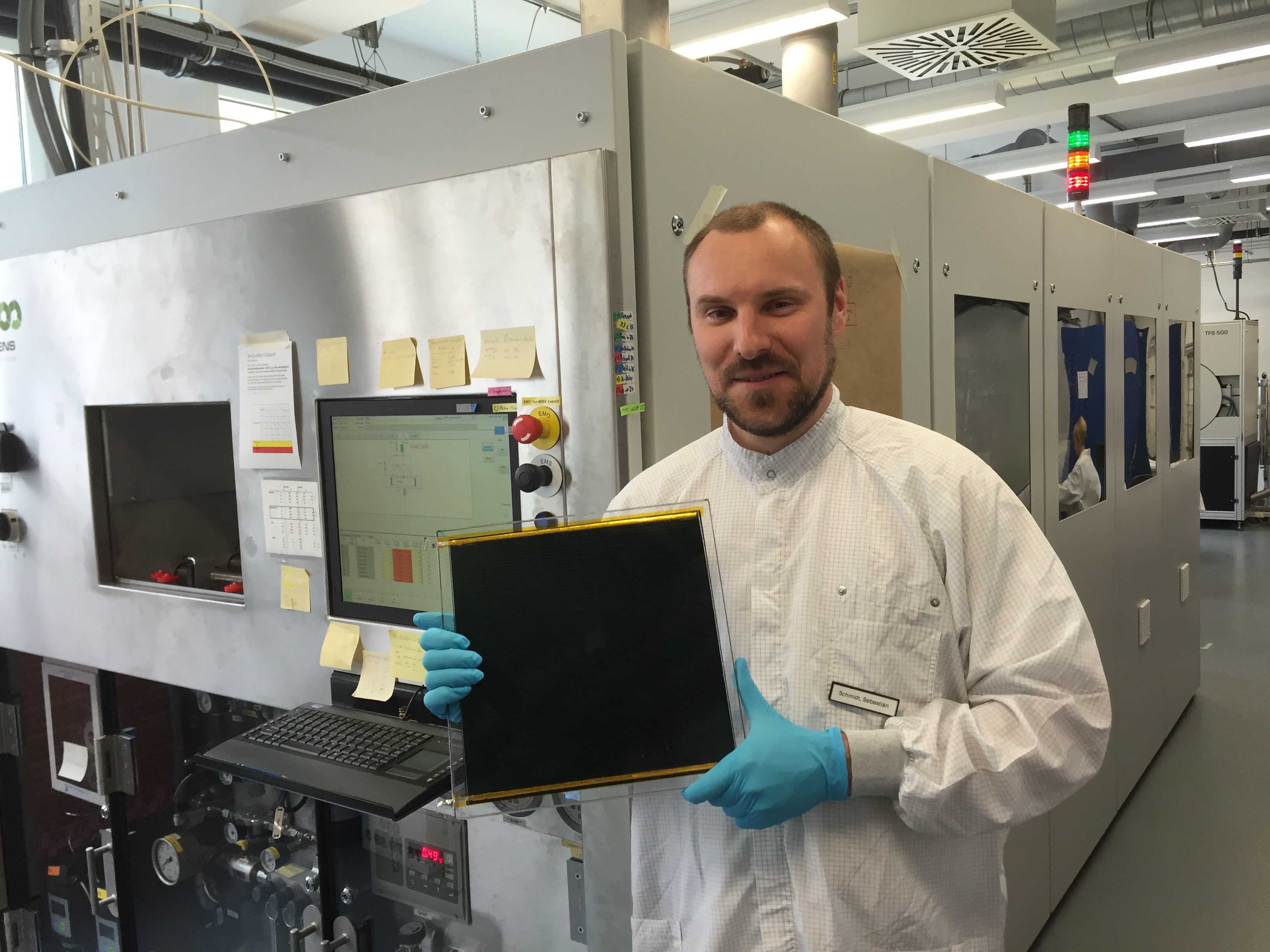
Dr. Sebastian Schmidt, project leader ACESS-CIGS
PVcomB has gained a large project for the further improvement of the manufacturing process for CIGS thin-film solar cells together with partners from Germany and the Netherlands. The atmospheric pressure process operates without involving toxic gases and will be more economical. It will run under the acronym ACCESS-CIGS, which stands for “Atmospheric European Cooperation in Science and Technology (COST) Competitive Elemental Sulpho-Selenisation for CIGS”.
Experts at the Competence Centre Thin-Film- and Nanotechnology for Photovoltaics Berlin (PVcomB) in Adlershof are developing an innovative process to fabricate CIGS layers for application in thin-film solar cells. CIGS stands for the compound Cu(In,Ga)(Se,S)2, consisting of copper, indium, gallium, selenium and sulphur. Polycrystalline CIGS solar cell technology is noted for its high efficiencies at the solar-cell level and high energy yields for solar modules.
The process pursued at PVcomB does not require a vacuum and utilises elementary selenium and sulphur to convert the metallic precursor layer of copper-indium-gallium to a polycrystalline CIGS semiconductor layer. This has the advantage that the process can be carried out without the use of toxic gases such as hydrogen selenide (H2Se), saving on production costs. This might permit the manufacture of CIGS solar modules to be considerably more economical and thus support the currently difficult market situation.
PVcomB has been successful in attracting funding of 800 000 EUR under the SOLAR-ERA.NET Initiative. Staff will be working on the technology as part of a bi-national European consortium over the next two years to optimise the addition of selenium and improve its influence on the crystallisation process.
The project will be carried out in cooperation with the companies TNO/Solliance and Smit Thermal Solutions, both located in Eindhoven, Netherlands, and with the firm Dr. Eberl MBE Komponenten in Weil der Stadt on the German side.