PVcomB
CIGS layers grown by multi-source evaporation
The PVcomB has been successful in developing CIGS preparation processes for high efficiency, taking into account compatibility with industrial production. These developments were aimed at stand-alone, single junction CIGS solar cells. but now form the basis for using the CIGS cell as a bottom cell in CIGS/pero tandems. Our preferred method for CIGS preparation is multi-source evaporation. The particular requirements for the tandem application are now the focus of our CIGS research and they include:
- A highly reproducible CIGS bottom cell baseline as a reliable basis for the complex tandem cell preparation
- High efficiency of the CIGS bottom cell under the long-wavelength illumination passing through the top cell
- Reduced roughness and low density of shunt-inducing morphological defects
- Quality control methods tailored to the tandem application
With these developments we participate in the national indu-bottomCIGS project.
Topics
Heavy Alkali Post Deposition Treatment of CIGS Absorbers
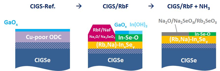
Fig. 1: Our current understanding of the working mechanism of a RbF post deposition treatment of a CIGS absorber
The RbF post deposition treatment was originally developed to increase the open circuit voltage and thereby efficiency of CIGS single junction solar cells. If not carried out correctly there is a risk of forming current transport barriers resulting in reduced fill factor. The thorough understanding that we had gained has helped us to keep the PDT also for preparing high efficiency bottom cells.
References
T. Kodalle, M. D. Heinemann, D. Greiner, H. A. Yetkin, M. Klupsch, C. Li, P. A. van Aken, I. Lauermann, R. Schlatmann, C. A. Kaufmann, Elucidating the Mechanism of an RbF Post Deposition Treatment in CIGS Thin Film Solar Cells, Solar RRL 2 (9), 1800156 (2018).
T. Kodalle, R. Kormath Madam Raghupathy, T. Bertram, N. Maticiuc, H. A. Yetkin, R. Gunder, R. Schlatmann, T. Kühne, C. A. Kaufmann, H. Mirhosseini, Properties of RbInSe2 thin films, Physica Status Solidi: Rapid Research Letters 1800564 (2018)
Alejandra Villanueva-Tovar, Tim Kodalle, Christian A. Kaufmann, Rutger Schlatmann, Reiner Klenk, Limitation of Current Transport across the Heterojunction in Cu(In,Ga)Se2 Solar Cells Prepared with Alkali Fluoride Postdeposition Treatment, Solar RLL 4 (2020)
Tim Kodalle; Hasan A. Yetkin; Alejandra Villanueva Tovar; Tobias Bertram; Reiner Klenk; Rutger Schlatmann, A Device Model for Rb-Conditioned Chalcopyrite Solar Cells, IEEE Journal of Photovoltaics 11 (2021)
Reproducible CIGS Preparation for High Efficiency Bottom Cells
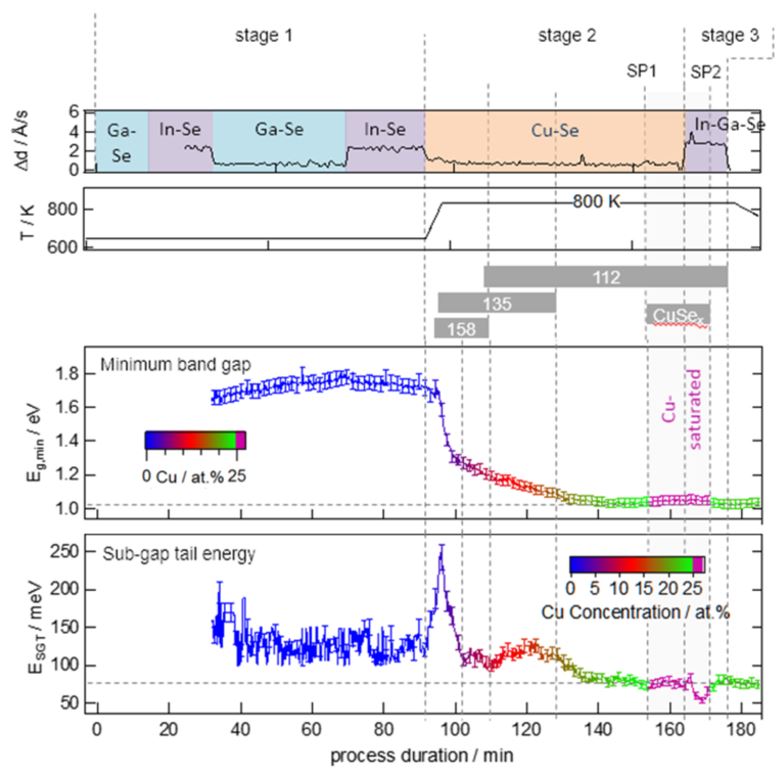
Fig. 2: Properties of the growing CIGSe thin film as observed via White Light Reflectometry (WLR) in real-time during 3-stage coevaporation: deposition rate from WLR, chalcopyrite phases (158 signifying Cu(In,Ga)5Se8, same for 135 and 112) from ED-XRD, Eg,min from WLR, ESGT from WLR, roughness (not shown) from WLR.
The preparation of the bottom cell CIGS film needs to be highly reproducible to form a solid basis for tandem developments. For optimum tandem cell efficiency, the effective band gap of the CIGS film needs to be narrower than for the single junction, which implies the need for a precise control of the Gallium and Indium grading in the film. For both requirements we rely on the previously developed three-stage process with in-situ optical process control using laser light that is scattered or infrared light that is reflected off the growing CIGS thin film. The correlation between optical and other properties of the growing film was established by a combination of white light reflectometry (WLR) and in-situ real-time EDXRD (Fig. 2) .
References
D. Greiner, J. Lauche, M.D. Heinemann et al., Proc. 43rd IEEE PVSC, Portland (2016) 1151-1156, doi:10.1109/PVSC.2016.7749795.
M.D. Heinmann, R. Mainz, F. Österle et al., Scientific Reports 7 (2017) 45463, doi:10.1038/srep45463.
Incorporation of Silver
The incorporation of small amounts of Silver into the CIGS films can help to reduce the required substrate temperature which is a prerequisite for certain flexible substrates. It may also help to establish a surface morphology which is more suitable for the subsequent growth of the top cell layers.
References
Sateesh Prathapani, Sevan Gharabeiki, Jakob Lauche, René Schwiddessen, Pablo Reyes-Figueroa, Nikolaus Weinberger, Michele Melchiorre, Rutger Schlatmann, Iver Lauermann, Christian Alexander Kaufmann, Impact of Minimal Silver Incorporation on Chalcopyrite Absorbers—Origins for Improved Open-Circuit Voltages in (Ag,Cu)(In,Ga)Se2 Solar Cells, Solar RRL (2025)
Flexible Substrates
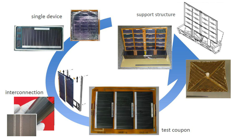
Fig. 4 In the development of a CIGSe based solar generator for space applications within a German consortium of academic and industrial partners the HZB studied absorber growth at low deposition temperatures on flexible polyimide foil substrates. [8]
From 2007 until 2015 a German consortium of academic and industrial partners, developed an extremely light and flexible Cu(In,Ga)Se2 (CIGSe) thin film solar cell technology for space applications. We build on this experience to develop CIGS/pero tandem cells and modules on flexible substrates. For this terrestrial application we are considering steel foil or ultra-thin bendable glass as flexible substrates and aim at monolithicallly interconnected modules.
References
C. A. Kaufmann, D. Greiner, S. Harndt et al., Proc. 29th EU PVSEC, Amsterdam (2014) 1439-1443, doi:10.4229/EUPVSEC20142014-3AO.5.4.
C. A. Kaufmann, D. Greiner, H. Rodriguez-Alvarez et al., Proc. 39th IEEE PVSC, Tampa (2013) 3058-3061, doi:10.1109/PVSC.2013.6745106.
D. Greiner, J. Lauche, S. Harndt et al., Proc. 42nd IEEE PVSC, New Orleans (2015) 1-6, doi:10.1109/PVSC.2015.7356149.