PVcomB
Silicon Based Tandem-Technologies for Industrial PV Applications
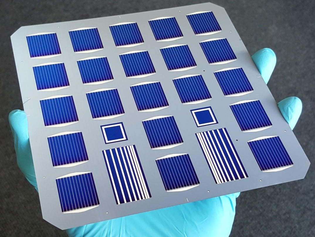
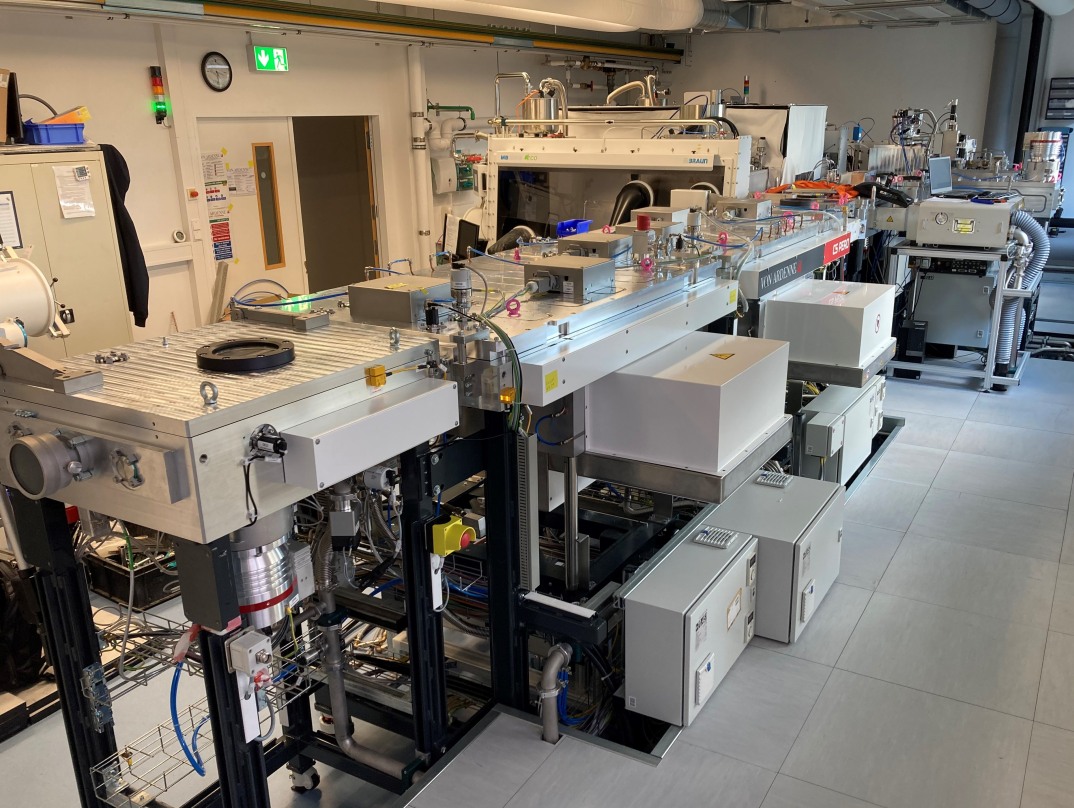
In the Tandem Industrialization Group at PVcomB, we bridge the gap between cutting-edge research and industrial application. Our goal is to develop and scale up silicon-based tandem solar cells, focusing on industrially relevant materials, processes, and technologies. Our group operates semi-automated, high-throughput, industrial-scale equipment, allowing us to efficiently transfer our findings to the photovoltaic industry. Processing capabilities include glass-based substrates up to 30 × 30 cm² and silicon wafers up to 166 × 166 mm² (M6 format).
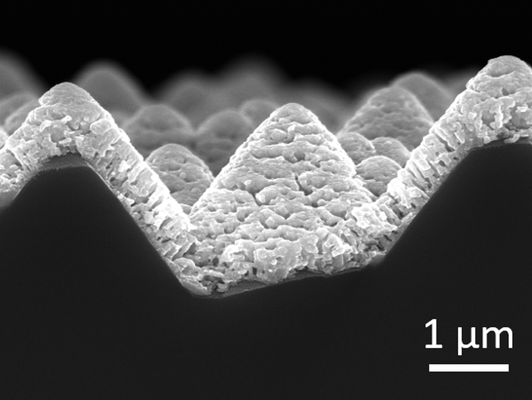
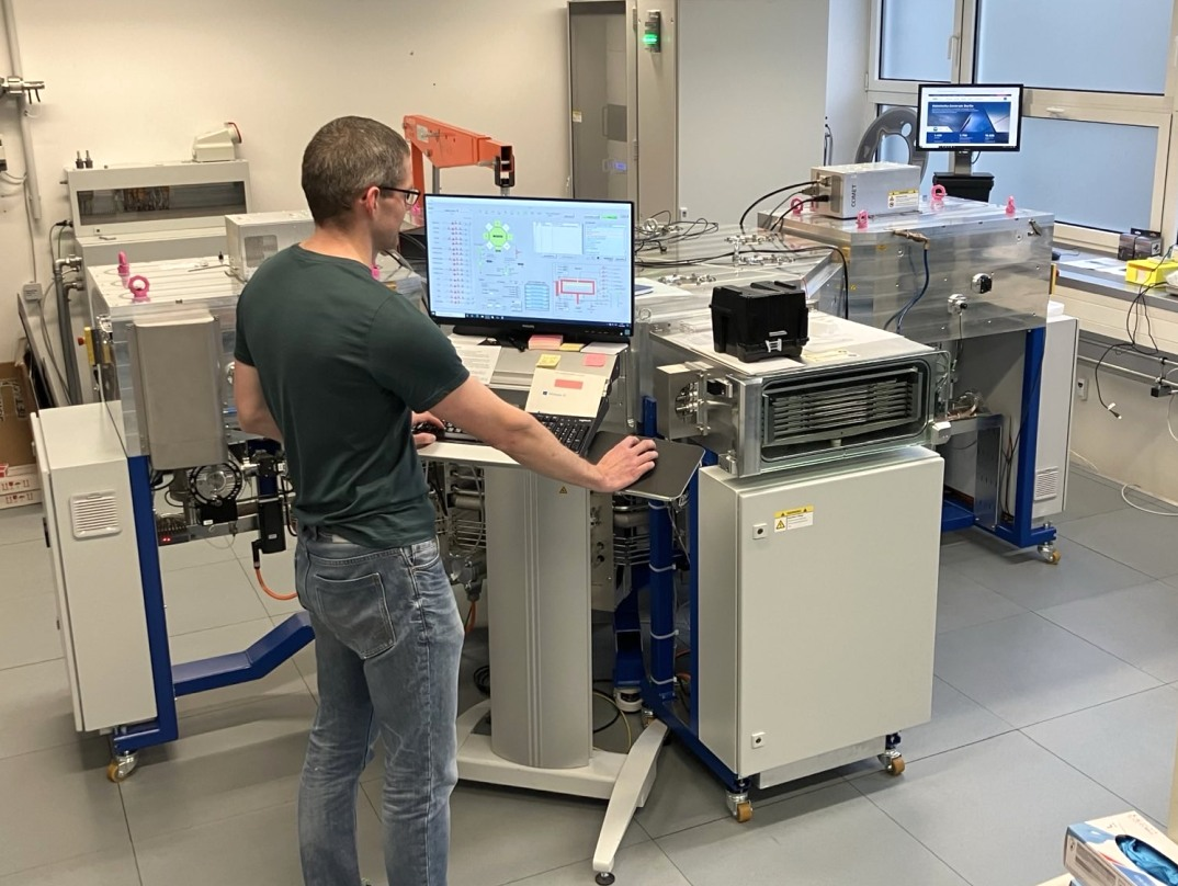
With a strong foundation in silicon photovoltaics, we have established a stable silicon heterojunction (SHJ) baseline over many years. This provides the perfect platform for the development of high-efficiency silicon/perovskite tandem solar cells. We can produce the perovskite solar cell in various ways: We have developed our KOALA system exclusively for evaporation processes (PVD). In addition, we are researching several scalable deposition techniques that are compatible with industrial processes. Our expertise spans the entire process chain, from as-cut silicon wafers to complete tandem devices, enabling comprehensive research and development.
Our team brings together scientists and engineers, working hand in hand to accelerate the transition from research to industry. We provide expertise in materials, processing, and device optimization, always with a focus on practical implementation.