EMIL
Thin Film and Nanostructured PV Materials
Photovoltaic (PV) technologies must sustain terawatt scale production and therefore require widely available, environmentally friendly base materials combined with highest conversion efficiencies at the lowest possible cost.
This, in turn, requires the design of materials, components, industrial processes and devices combined with the dedicated analysis, modeling, and control of each step within the production and life cycle of the solar module. Besides Si-based PV which dominates the market today other PV technologies based on different absorber materials such as compound semiconductors, perovskites, light-absorbing dyes, organic materials, or quantum dots are being developed, offering advantages over Si-based PV such as higher efficiency or compatibility with flexible substrates, but suffer from disadvantages such as higher costs or lower efficiency.
Highlighted topics:
- Band structure of highly doped oxides
- Novel contact system for silicon-based solar cells and related devices
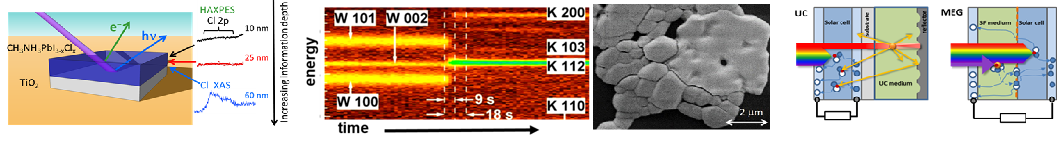
- Photovoltaic absorber film formation via metastable nanocrystals
- Tailored kesterite nanoparticles fabrication for improved solar energy conversion
- Film growth study by real-time XPS +XRD
- Interface chemistry and contacts formation in thin film solar cells
- In-situ monitoring of formation/degradation of hybrid perovskite materials
- Lead-free hybrid perovskite absorber materials
- Deriving the composition profile in perovskites
- Organic spectral conversion for solar energy applications