Anwendungsbeispiele
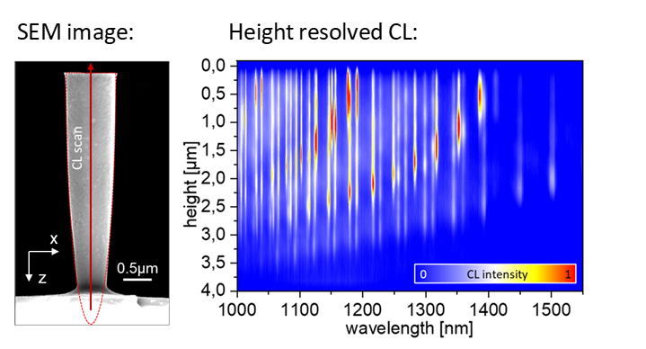
Cathoduluminescence : Direct measurement and analytical description of the mode alignment in inversely tapered silicon nano-resonators
Inversely tapered silicon photonic resonators on silicon substrates were shown to host multiple high–Q whispering gallery modes and constitute versatile building blocks for CMOS compatible solid state lighting, optical sensing and modulator devices. In this application the cathodoluminescence signal in the infrared spectral range was mapped along the long vertical axis of a Si nanoresonator. The analysis shows that the observed whispering gallery modes could indeed be excited very locally by the electron beam and that the main spectral features can be explained by a pure geometric model considering the refractive index of Si.
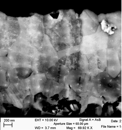
SEM image depicting the microstructure of a
Cu(In,Ga)Se2 thin film
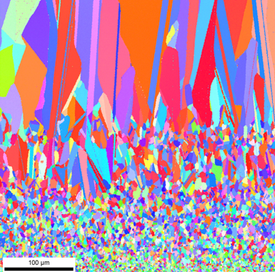
EBSD orientation distribution map of Si thin film
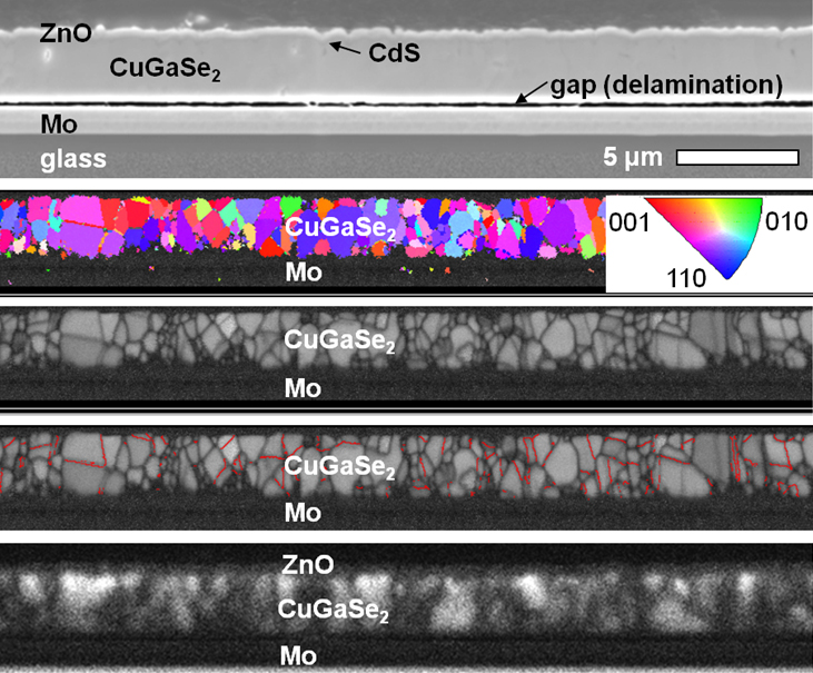
SEM image EBSD orientation distribution and pattern-
quality maps, also with Σ3 grain boundaries highlighted
by red lines as well as a panchromatic CL image, all acquired
at the identical position of a ZnO/CdS/ CuGaSe2/Mo/glass
cross-section specimen (see also: Abou-Ras et al.,
Sol. En. Mat. Sol. Cells 95 (2011) 1452)
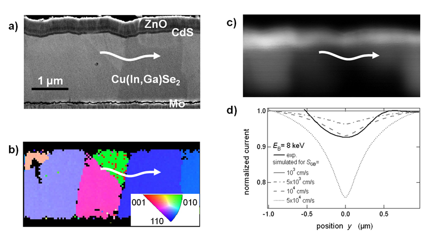
SEM image (a), EBSD orientation-distribution map (b) with local orientations given by colors
(see legend), and EBIC image acquired at 8 keV (c) on the identical sample position of a
polished cross-section of a Cu(In,Ga)Se2 thin-film solar cell. The white arrows indicate the
position of the extracted EBIC profiles shown in (d). See also: Nichterwitz et al., Thin Solid Films
517 (2009) 2554.
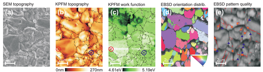
Combined SEM (a), KPFM (b+c) and EBSD analyses (d+e) of grain boundaries in CuInSe2 thin film.
See also: R. Baier et al., Appl. Phys. Lett. 99 (2011) 172102