Department Spin and Topology in Quantum Materials
in-operando Angle-Resolved Photoemission Spectroscopy (ioARPES)
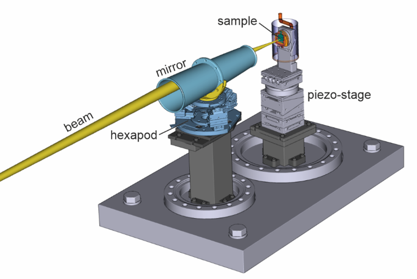
A new instrument "ioARPES" shall be constructed at a new branch of U125_PGM undulator. The project addresses the challenge of integrating a nanofabricated “laboratory-on-a-chip” into an ARPES experiment that enables both live Fermi-surface mapping during parameter changes and recording of the complete bandstructure with meV-resolution for μm-sized devices including complete 3D spin analysis of the photoelectrons. The spatial resolution will be realized by a <5 μm-sized beam focused onto a piezo-driven x-y-scanned sample stage. The sample stage will be constructed in a modular way with in-operando tuning capabilities of several stimuli such as current, electrostatic gating, strain, and electric fields. To vary parameters quickly, a novel faster analyzer for "live" probing of the Fermi surface (FeSuMa) will be used.
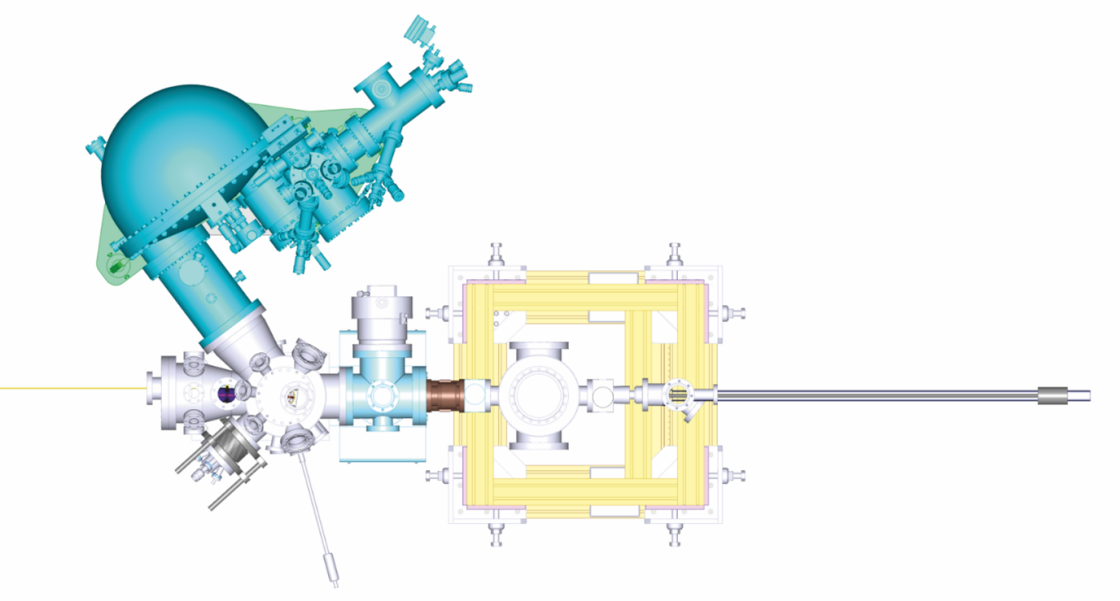
ioARPES station layout (top view)
Scientific aim
The scientific aim is to control multiple experimental “knobs” in the ARPES experiment such as:
Carrier density: Electrostatic gating controls the carrier density inside the material and hence its Fermi energy. Depending on these parameters, materials can change controllably their state and transition between insulating, metallic (e. g., black phosphorus), and correlated phases such as magnetic or superconducting ones (e. g., multilayer graphene, MoS2, cuprates).
Out-of-plane electric field: An out-of-plane electric field can be applied to 2DMs in a double-gated field effect transistor geometry via the difference in potentials between the top and the bottom gates.
In-plane electric field: Strong in-plane fields applied between source and drain electrodes at small distance across the 2DM create sizable non-equilibrium carrier distributions. These distributions can lead to phase transitions such as metal-insulator transitions or a breakdown of superconductivity, symmetry breakings, or to complex distributions of carriers in real and momentum space, e. g. via spin or orbital Hall effects.
Temperature: A central parameter is temperature aimed to be down to 10 K at the sample. This enables an energy resolution of 2-3 meV. The high energy resolution shall be used e.g. for probing emergent energy gaps as in the superconducting phases of gated 2DMs such as twisted bilayer graphene. It is also crucial to change temperature quickly searching for sweet spots in the parameter space. For this purpose, we will use a technology that can switch between room and cryogenic temperatures in minutes via on-chip current pulses.
Strain: Mechanical strain affects the bandgap size, energy hierarchy between different high symmetry points in momentum space, phonon dispersions, and electron-phonon couplings. Uniaxial strain can be used to break symmetries and to induce, e.g., couplings between various excitonic states. To develop ARPES-compatible strained samples, we will use the geometry with a gate voltage applied between a silicon substrate and a 2DM suspended over a circular cavity generates a pulling force for stressing the material.
Partners
The project is carried out in collaboration with RWTH Aachen University, Dresden University of Technology, Leibniz Institute for Solid State and Materials Research Dresden, Free University of Berlin.