Department Microstructure and Residual Stress Analysis
Experimental setup for in-situ EDXRD/XRF at BESSY II
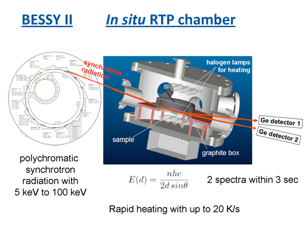
In-situ RTP (rapid thermal processing) chamber.
To study thin-film reactions under well defined and flexible conditions, we run three RTP (rapid thermal processing) chambers for sequential synthesis of Cu(In,Ga)Se2, Cu2ZnSnSe4, and Cu2ZnSnS4, and a PVD (physical vapour deposition) chamber developed to study multi-stage co-evaporation processes for the deposition of high-efficiency Cu(In,Ga)Se2 solar cell absorbers.
All chambers are tailor made for in situ investigations at the EDDI beamline of the synchrotron facility BESSY II of the HZB. During in situ measurements, polychromatic synchrotron radiation enters the chambers through a polyimide window and hits the sample under a shallow angle. The diffracted radiation as well as fluorescence radiation is simultaneously detected under one or two fixed angles by one or two energy-dispersive, high-purity Ge detectors.
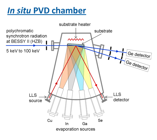
In-situ PVD (physical vapour deposition) chamber.
With this setup we are able to measure simultaneously and in real-time unique combination of film properties during thin film solid state reaction processes. These properties encompass:
- Phase formation (determined from diffraction signals) [1]
- Evolution of elemental depth distributions (by multi-angle diffraction
- and fluorescence) [2]
- Formation of macroscopic mechanical stress (by multi-angle diffraction) [3]
- Absorption and desorption of material (from fluorescence signals) [4]
- Evolution of crystallite sizes (from the profile of diffraction signals) [5,6]
- Changes of texture (by multi-angle diffraction)
Currently, we are setting up a novel in-situ X-ray laboratory equipped with a high-flux metaljet X-ray source and a 2D detector.
[1] R. Mainz, R. Klenk and M. Lux-Steiner. Thin Solid Films 515, 5934-5937 (2007), doi: 10.1016/j.tsf.2006.12.167.
[2] R. Mainz and R. Klenk. J. Appl. Phys. 109, 123515 (2011), doi: 10.1063/1.3592288.
[3] C. Genzel, I. A. Denks, R. Coelho, D. Thomas, R. Mainz, D. Apel and M. Klaus. Journal of Strain Analysis for Engineering Design 46, 615-625 (2011), doi: 10.1177/0309324711403824.
[4] A. Weber, R. Mainz and H. W. Schock. J. Appl. Phys. 107, 013516 (2010), doi: 10.1063/1.3273495.
[5] H. Rodriguez-Alvarez, R. Mainz, B. Marsen, D. Abou-Ras and H. W. Schock. J. Appl. Cryst. 43, 1053-1061 (2010), doi: 10.1107/S0021889810025860.
[6] D. Thomas, R. Mainz, H. Rodriguez-Alvarez, B. Marsen, D. Abou-Ras, M. Klaus, C. Genzel and H.-W. Schock. Thin Solid Films 519, 7193-7196 (2011), doi: 10.1016/j.tsf.2010.12.229.