Institute Solar Fuels
Devices
Introduction
Recent developments in solar fuels have resulted in a number of stand-alone solar water splitting devices. These efforts have resulted in an impressive 30% solar-to-hydrogen (STH) efficiency, albeit being achieved by combining expensive high-quality PV-grade III-V solar cells and precious metal catalysts. On the other hand, much lower efficiencies (5-10%) have only been reported from devices based on cheap abundant materials (e.g., Si, transition metal oxides). This efficiency-cost trade-off remain to be a challenge that needs to be addressed, along with scale-up design architecture that allows efficient heat, mass, and charge transport. Although novel architectures have been reported, three configurations are generally considered: (1) modular devices containing of separate photovoltaic (PV) cells connected to (dark) electrocatalysts (i.e., PV-electrolysis), (2) integrated photoelectrode devices, either with direct semiconductor/liquid junction or buried junction (i.e., PEC), and (3) dispersed photocatalyst particles in liquid electrolyte reactors (i.e., PC). Overall, the goal is to fabricate a solar water splitting device that produces hydrogen with a cost of less than 3 USD / kg (US DOE target).
Our approach
Tandem Device for Solar Water Splitting
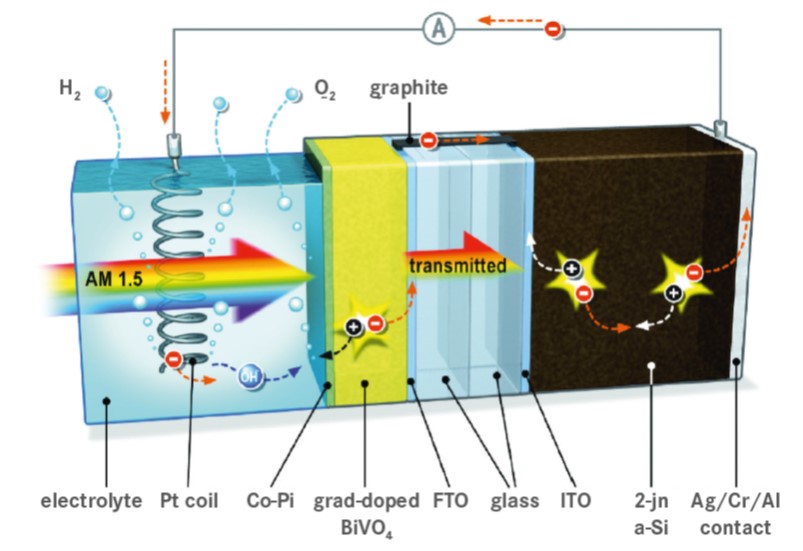
In Institute for Solar Fuels, we employ a tandem configuration where two semiconductor materials with different bandgaps are used to absorb the sunlight. The large bandgap semiconductor absorbs the short wavelength part (high photon energy) of the solar spectrum, while the long wavelength part (low photon energy) are transmitted. The small bandgap semiconductor can then utilize this transmitted spectrum. This way, not only that we open up the possibilities for more materials to be employed as photoelectrodes, we also utilize the solar spectrum more efficiently. In this research area, we are looking into combining multiple cheap, abundant materials as large- and small-bandgap semiconductors. As the large-bandgap semiconductor, we focused on novel absorbers (e.g., oxides, sulfides, see “Light Absorbers” section), whereas silicon is typically used as the small-bandgap semiconductor.
©HZB/Abdi
Highlights
We submitted a patent application to the Deutches Patent- und Markenamt for “Method of Surface Treatment of TCOs and Metal Oxides”. This method allowed us to overcome the Ohmic losses in our large scale photoelectrodes.
©HZB/Abdi
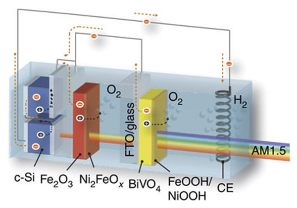
Together with our Korean collaborators (UNIST and POSTECH), we reported a 7.7 % STH efficiency solar water splitting device based on BiVO4, Fe2O3, and c-Si.
Read more: J. H. Kim, J.-W. Jang, Y. H. Jo, F. F. Abdi, Y. H. Lee, R. van de Krol, J. S. Lee, Hetero-type Dual Photoanodes for Unbiased Solar Water Splitting with Extended Light Harvesting, Nature Communications, 7:13380, 2016, 1-9
©HZB/Abdi