Institute Solar Fuels
Nanostructures
Nanostructures
The types of metal oxide semiconductor materials that are typically used as light absorbers in photoelectrochemical devices have a charger carrier transport length (≤ 100 nm) that is much shorter than the light penetration depth (200 - 500 nm). This can lead to excessive recombination of photo-generated carriers and low overall efficiency. One way to circumvent this mismatch between the charge carrier transport length and light penetration depth is by incorporating nanostructures into photoelectrochemical devices. This includes adding nanostructure to the absorber layer and/or using a nanostructured transparent conducting oxide scaffold under the absorber layer. We are currently collaborating with different groups on nanostructure projects and developing new systems to make nanostructures on our own.
Highlights
Collaboration with Max Planck Institute of Colloids and Interfaces, Joef Stefan Institute, Department for Nanostructured Materials, and Ben-Gurion University of the Negev resulted in a paper.
- Špela Hajduk, Sean P. Berglund, Matejka Podlogar, Goran Draić, Fatwa F. Abdi, Zorica C. Orel, Menny Shalom, “Conformal Carbon Nitride Coating as an Efficient Hole Extraction Layer for ZnO Nanowires-based Photoelectrochemical Cells,” Advanced Materials Interfaces - accepted
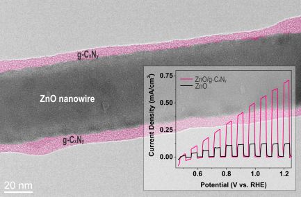
©HZB/Berglund
Supplier quotations have been received for the new glancing angle deposition (GLAD) system, which will be used for depositing nanostructured thin films. It will be part of HEMF and available to internal and external users.
Link to HEMF project: http://www.helmholtz-berlin.de/projects/hemf