Department Interface Design
Examples from Current Research
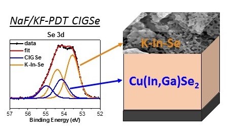
Investigating the Alkali Postdeposition Treatment of Cu(In,Ga)Se2 Thin-Film Solar Cell Absorbers
We have investigated the effects of alkali fluoride postdeposition treatments (PDT) on the chemical and electronic surface and near-surface structure of Cu(In,Ga)Se2 (CIGSe) absorbers using a variety of x-ray based spectroscopies. Laboratory-based x-ray photoelectron spectroscopy (XPS) and synchrotron-based hard x-ray photoelectron spectroscopy (HAXPES) have been used to determine the surface and near-surface composition of the absorbers, which significantly changes depending on the performed postdeposition treatments focusing on the influence of NaF and NaF/KF-PDT when compared to alkali-free (i.e. untreated) CIGSe absorbers. The alkali-free and NaF-PDT absorbers show similar chemical properties, having a Cu and Ga poor surface region compared to the nominal bulk and the same chemical environment for indium and selenium. For the NaF/KF-PDT samples a K-In-Se compound is present on top of a Cu-In-Ga-Se compound, with a nanopatterned surface. Synchrotron-based x-ray emission spectroscopy (XES) and x-ray absorption spectroscopy (XAS) have been used to also probe the chemical environment of selenium and potassium. Based on the comparison of the spectra of the untreated (alkali-free) and the NaF-PDT CIGSe absorber, we find no significant change in the Se environment. However, the spectrum of the NaF/KF-PDT CIGSe absorber indicates the presence of a different Se species. Both, the Se and K related spectra of the NaF/KF-PDT CIGSe sample, are in good agreement with the spectra of a KInxSey-like compound.
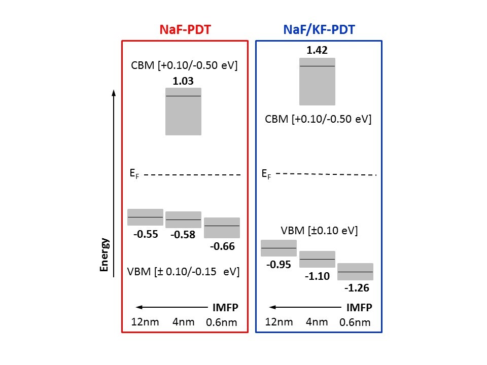
HAXPES was also used to depth-dependently study the valence band together with ultraviolet photoelectron spectroscopy (UPS). Inverse photoemission was employed to derive the conduction band minimum (CBM). For the NaF/KF-PDT CIGSe absorber, we find a significant shift of the valence band maximum (VBM) and CBM away from the Fermi level compared to the alkali-free and NaF-PDT CIGSe, resulting in a significantly increased surface band gap of 2.52 (+0.14/-0.51) eV. This is in agreement with a Cu- and Ga-devoid surface region and the formation of a K-In-Se surface compound Furthermore, we find that for all measurements and all samples the VBM moves away from the Fermi level with increasing surface sensitivity, indicating chemically and/or electronically modified CIGSe surfaces.
For more details see:
E. Handick, P. Reinhard, J.-H. Alsmeier, L. Köhler, F. Pianezzi, S. Krause, M. Gorgoi, E. Ikenaga, N. Koch, R. G. Wilks, S. Buecheler, A. N. Tiwari, and M. Bär, Potassium Postdeposition Treatment-Induced Band Gap Widening at Cu(In,Ga)Se2 Surfaces – Reason for Performance Leap?, ACS Appl. Mater. Interfaces 7, 27414 (2015)
E. Handick, P. Reinhard, R. G. Wilks, F. Pianezzi, T. Kunze, D. Kreikemeyer-Lorenzo, L. Weinhardt, M. Blum, W. Yang, M. Gorgoi, E. Ikenaga, D. Gerlach, S. Ueda, Y. Yamashita, T. Chikyow, C. Heske, S. Buecheler, A. N. Tiwari, and M. Bär, Formation of a K—In—Se Surface Species by NaF/KF Postdeposition Treatment of Cu(In,Ga)Se2 Thin-Film Solar Cell Absorbers, ACS Appl. Mater. Interfaces 9, 3581 (2017)
Direct Observation of an Inhomogeneous Chlorine Distribution in CH3NH3PbI3-xClx Layers: Surface Depletion and Interface Enrichment
We have used hard X-ray photoelectron spectroscopy (HAXPES) at different photon energies and fluorescence yield X-ray absorption spectroscopy (FY-XAS) to non-destructively investigate CH3NH3PbI3-xClx perovskite thin films on compact TiO2. This combination of spectroscopic techniques allows the variation of information depth from the perovskite layer surface to the top-most part of the underlying compact TiO2 layer. We have taken advantage of this to understand the distribution of chlorine throughout the perovskite/TiO2 layer stack. No Cl is detected using HAXPES, indicating surface depletion of Cl and allowing us to place an upper limit on the amount of Cl in the perovskite layer: x < 0.07 and x < 0.40 to depths of ~10 nm and ~26 nm, respectively, beneath the perovskite film surface. Our FY-XAS results, however, demonstrate that there is a higher average concentration of Cl throughout the perovskite layer than at the surface (x > 0.40) consistent with both enhanced concentrations of Cl deep beneath the perovskite film surface and near the CH3NH3PbI3-xClx perovskite/TiO2 interface. The consequences of this distribution of Cl in the CH3NH3PbI3-xClx perovskite layer on device performance are discussed.
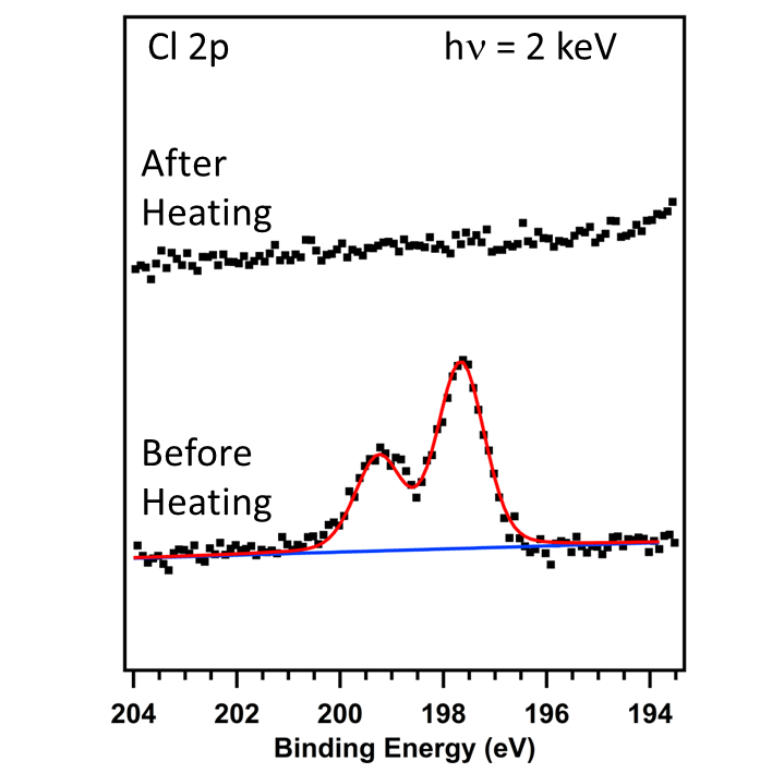
Cl 2p spectra taken with a photon energy of 2 keV of a 3 : 1 mole ratio, CH3NH3I : PbCl2, solution in DMF, drop-cast onto a compact TiO2 layer and dried in UHV; at room temperature before heating (bottom), after heating to 140 °C (top).
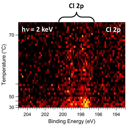
The Cl 2p region as a function of temperature taken with a photon energy of 2 keV. Yellow indicates higher intensities in the plot. The Cl 2p region is indicated at the top of the plot.
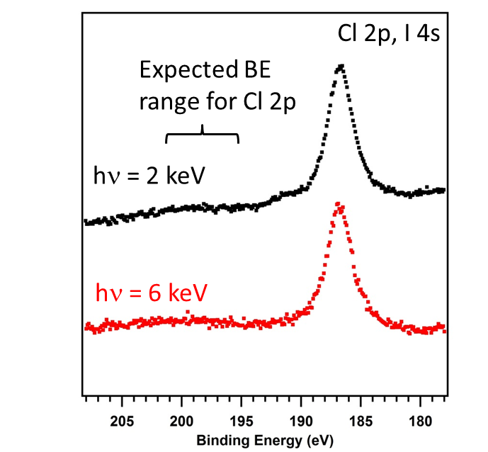
Cl 2p and I 4s spectra taken with a photon energies of 2 keV (black) and 6 keV (red) of a 60 nm thick CH3NH3PbI3-xClx film on compact TiO2. Note the absence of any detectable Cl in both spectra.
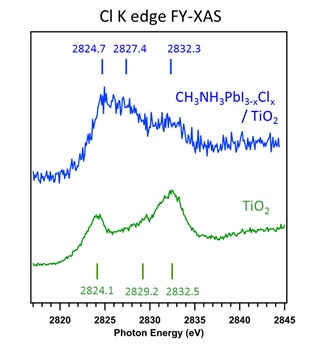
Cl K edge FY-XAS spectra of a 60 nm thick CH3NH3PbI3-xClx layer on compact TiO2 (blue) and the compact TiO2 layer without a CH3NH3PbI3-xClx layer on top (green). Note the distinctively different shapes of the two spectra.
For more details see:
D.E. Starr, G. Sadoughi, E. Handick, R.G. Wilks, J.H. Alsmeier, L. Köhler, M. Gorgoi, H.J. Snaith, and M. Bär, Direct observation of an inhomogeneous chlorine distribution in CH3NH3PbI3−xClx layers: surface depletion and interface enrichment, Energy Environ. Sci. 8, 1609 (2015)
The impact of Cu2-xS surface phases and their impact on the electronic structure of CuInS2
Combining surface and near-surface bulk sensitive x-ray spectroscopies to study CuInS2 (CIS) thin-film solar cells absorbers, we could identify spatially separated areas with different surface properties. The dark and light areas (distinguishable by eye before KCN etching) are dominated by CuS and Cu2S like secondary surface phases. After the removal of the Cu2−xS phases by KCN etching the CIS samples appear similar to the eye but the surface composition still signifficantly differs; in particular in the degree of Cu-deficiency. We also see a change in the surface band gap (see publication for details). Such (hidden) inhomogenieties might be an explanation why respective solar cells fall behind compared to their low-gap counterparts w.r.t. device performance.
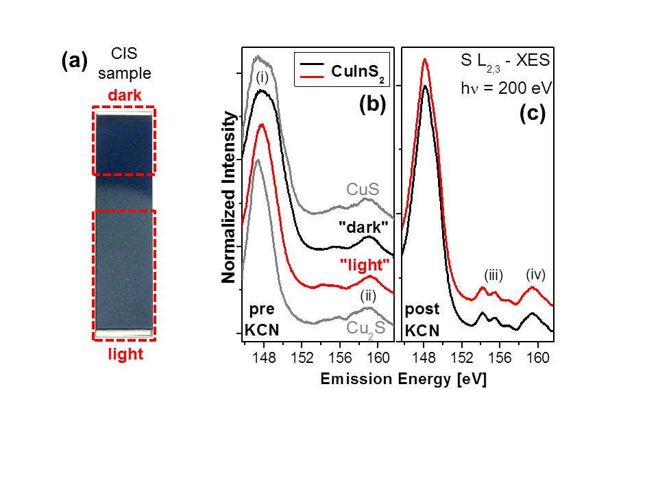
(a) Photograph of a CIS sample (½ inch × 2 inch). (b,c) S L2,3 XES spectra of dark (black spectra) and light (red spectra) CIS material before (b) and after (c) KCN etch. For comparison, the spectra of CuS and Cu2S are shown. The dark area appears to be CuS like while the light area shows more similarity to Cu2S. After the KCN etch the chemical environment of the S atoms in the near-surface bulk of the two samples as their appearance to the eye (not shown) is very similar.
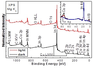
XPS survey spectra of initially dark and light CIS material after KCN etching. Inset: Respective XPS spectra of the valence band region compared to that of an In2S3 reference. We observe a significant variation of the Cu 3p line intensity, indicating a change in the In/Cu surface ratio of the two CIS samples. By fitting the respective peaks, we are able to reveal that while a Cu deficiency is found at the surface of both samples, it is significantly more pronounced for the (initially) light CIS sample.
For more details see:
M.Bär, J. Klaer, L. Weinhardt , R.G. Wilks, S. Krause, M. Blum, W. Yang, C. Heske, and H.-W. Schock, Cu2-xS Surface Phases and Their Impact on the Electronic Structure of CuInS2 Thin Films – A Hidden Parameter in Solar Cell Optimization, Adv. Energy Mater. 3, 777 (2013)
Si-O formation at the Si/ZnO thin-film solar cell interface
State-of-the-art thin-film silicon solar cells often feature ZnO:Al as a transparent window layer. Hard x-ray photoelectron spectroscopy (HAXPES) was used to investigate the resulting buried Si/ZnO interface. It was found that the solid phase crystallization (SPC) of the (initially) amorphous silicon leads to an (additional) formation of Si-O bonds at the Si/ZnO interface. Furthermore, the ZnO could be identified as the oxygen source for this process. Altogether, this may shed new light on why solar cells based on Si/ZnO layer stacks fall behind w.r.t. the expected device efficiencies.
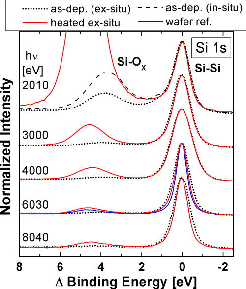
Si 1s photoemission spectra for excitation energies (hν) ranging from 2 to 8 keV before (black) and after a SPC heat treatment. The two main emission features can be attributed to Si-Si and Si-Ox bonds, respectively. The slightly narrower Si-Si emission line can be explained with the transformation of amorphous silicon into polycrystalline silicon. The strong post-SPC increase of the Si-Ox related signal clearly indicates a Si (surface) oxidization when doing the SPC ex-situ.
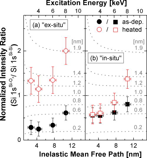
Si 1sSi–Ox/Si 1sSi–Si intensity ratio of the Si/ZnO layer stack compared to that of a reference system in which Si–OX bonds are exclusively present at the surface (an oxidized Si wafer).for ex-situ (a) and in-situ (b) SPC-treated samples. The increase of this intensity ratio with increasing excitation energy (i.e., inelastic mean free path) does not agree with the behavior predicted by the surface oxidation model (dotted grey lines) and thus can be interpreted as a strong indication of an oxidation at the Si/ZnO interface.
For more details see:
M. Wimmer, M. Bär, D. Gerlach, R.G. Wilks, S. Scherf, C. Lupulescu, F. Ruske, R. Felix, J. Hüpkes, G. Gavrila, M. Gorgoi, K. Lips, W. Eberhardt, and B. Rech, Hard x-ray photoelectron spectroscopy study of the buried Si/ZnO thin-film solar cell interface: Direct evidence for the formation of Si–O at the expense of Zn-O bonds, Appl. Phys. Lett. 99, 152104 (2011).
Band alignment at the CdS/Cu2ZnSnS4 thin-film solar cell heterojunction
Earth-abundant Cu2ZnSnS4 (CZTS) kesterites are promising absorbers for thin-film solar cells. A combination of direct and inverse photoelectron spectroscopy was used to study the band alignment at the CdS/CZTS interface. A cliff-like conduction band offset was revealed and a significant etch-induced enhancement of the energetic barrier for charge carrier recombination across the CdS/CZTS interface was found.
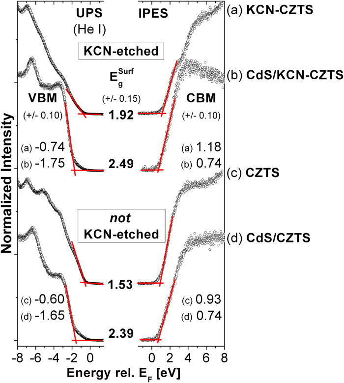
UPS (left) and IPES (right) spectra of (a) the KCN-CZTS, (b) the CdS/KCN-CZTS, (c) the CZTS, and (d) the CdS/CZTS sample surfaces. The linear extrapolation (red solid lines) of the leading UPS and IPES edges to determine VBM and CBM, respectively, is indicated. The determined surface band gap, , of the absorber layer is significantly increased after KCN-etching. The “cliff-like” conduction band offset at the CdS/CZTS interface, however, remains the same within measurement accuracy (see also the figure on the right-hand side).
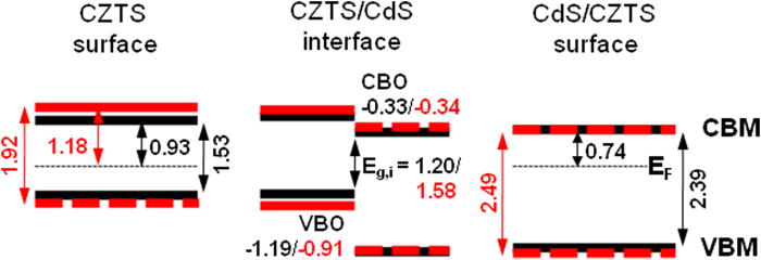
Schematic presentation of the band positions at the kesterite and CdS/kesterite sample surfaces and resulting band alignment at the interface. The red schemes and numbers represent the situation for the KCN-etched CZTS absorber. The experimental uncertainty for the VBM and CBM is ± 0.10 eV, and that for the Egsurf and interface band gap Eg,i values is 0.15 eV.
For more details see:
M. Bär, B.-A. Schubert,, B. Marsen, R. G. Wilks, S. Pookpanratana, M. Blum, S. Krause, T. Unold, W. Yang, L. Weinhard, C. Heske, and H.-W. Schock, Cliff-like conduction band offset and KCN-induced recombination barrier enhancement at the CdS/Cu2ZnSnS4 thin-film solar cell heterojunction, Appl. Phys. Lett. 99, 222105 (2011).
Depth-resolved band gap in Cu(In,Ga)(S,Se)2 thin films
The surface composition of Cu(In,Ga)(S,Se)2 (“CIGSSe”) thin films intrinsically deviates from the corresponding bulk composition, which also modifies the electronic structure and thus the optical properties. We used a combination of photon and electron spectroscopies with different information depths to gain depth-resolved information on the band gap energy (Eg) in CIG(S)Se thin films. We find an increasing Eg with decreasing information depth, indicating the formation of a surface region with significantly higher Eg. This Eg-widened surface region seems to extend further into the bulk of the sulfur-free CIGSe thin film compared to the CIGSSe thin film.

Left: optical reflection spectra of CIGSe (top) and CIGSSe (bottom) thin films, together with the respective envelopes of the interference extrema and the constructed mean values (red dotted lines). Insets: Eg determination (±0.05 eV) using an approximated absorption coefficient for the CIGSe (top) and CIGSSe (bottom) samples.
Center: Cu L3 XES (left) and XAS (right) spectra of the investigated CIGSe (middle spectra) and CIGSSe (bottom spectra) samples and of a metallic Cu reference (top). The band gap energies “Eg” (i.e., lower bounds for the true band gap values) are determined by linear extrapolation of the leading edges (±0.20 eV), indicated by the solid green and red lines.
Right: UPS (left) and IPES (right) of the CIGSe (top) and CIGSSe (bottom) samples. Spectra are shown for the as-introduced (thin solid lines) and for the cleaned samples (dots). The solid green and red lines indicate the linear extrapolation of the leading edges to determine Eg (±0.15 eV).
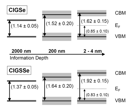
Schematic presentation of the determined CIGSe (top) and CIGSSe (bottom) band gap energies using the three different spectroscopic approaches (optical reflection, left; XES and XAS, center; UPS and IPES, right). The respective information depths of the applied spectroscopies are also shown. The gray area represents the measurement error. CBM (VBM) denotes the conduction band minimum (valence band maximum).
For more details see:
M. Bär, S. Nishiwaki, L. Weinhardt, S. Pookpanratana, O. Fuchs, M. Blum, W. Yang, J.D. Denlinger, W.N. Shafarman, and C. Heske, Depth-resolved band gap in Cu(In,Ga)(S,Se)2 thin films, Appl. Phys. Lett. 93, 244103 (2008).