Department Interface Design
Combined approach to analysis and optimization in thin-film PV technology
Young Investigator Group Interface Design
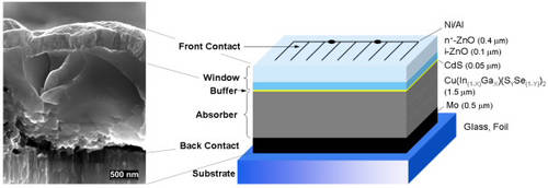
In recent years, thin film photovoltaics have exhibited rapid and impressive development. Today’s thin film photovoltaic systems are on the verge of commercialization, superseding the (more expensive) current state-of-the-art wafer-based Si solar cell technology. One of the main challenges for the development of high-efficiency thin-film solar cells is to understand the structure-function relationship of materials and their interfaces with the ultimate aim of tailoring material growth/preparation and interface formation to increase power conversion efficiencies and reduce production costs. Common empirical trial-and-error approaches reach their limits for complex multi-layered thin-film structures as employed in PV applications. Since the interfaces play a key role in such devices, the key issue for a knowledge-based approach to material and device development is to determine the chemical and electronic structure of these interfaces.
To tackle this complex challenge, the Young Investigator Group proposes an interdisciplinary four-pillar approach:
- Study the performance and the electronic characteristics of the solar cell device.
- Examine the initial chemical and electronic interface structure (e.g., band offsets, charge carrier dynamics...).
- The information gained from 1 and 2 is used to develop and improve upon models that can describe the "real-world" devices under investigation, with the goal of determining the identities and properties of the performance-limiting interfaces, leading to the final pillar:
- Recommend and employ deliberate surface/interface modifications to systematically tailor the electronic structure in order to reduce/avoid loss processes.
The goal of the Young Investigator Group is to develop and establish this analysis/optimization approach resulting in an insight-driven rapid progress in thin-film PV technology.